Semiconductor package structure and manufacturing method thereof

A technology of packaging structure and manufacturing method, which is applied in semiconductor/solid-state device manufacturing, semiconductor devices, semiconductor/solid-state device components, etc., and can solve problems such as structural strength influence and carrier reduction

Inactive Publication Date: 2017-06-09
CHIPMOS TECH INC
View PDF8 Cites 0 Cited by
  • Summary
  • Abstract
  • Description
  • Claims
  • Application Information

AI Technical Summary

Problems solved by technology

However, the thickness reduction of the carrier is limited and will affect its structural strength

Method used


Image

  • Semiconductor package structure and manufacturing method thereof
  • Semiconductor package structure and manufacturing method thereof
  • Semiconductor package structure and manufacturing method thereof

Examples


Embodiment Construction

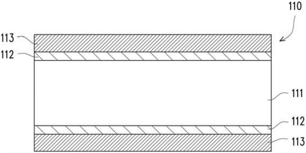
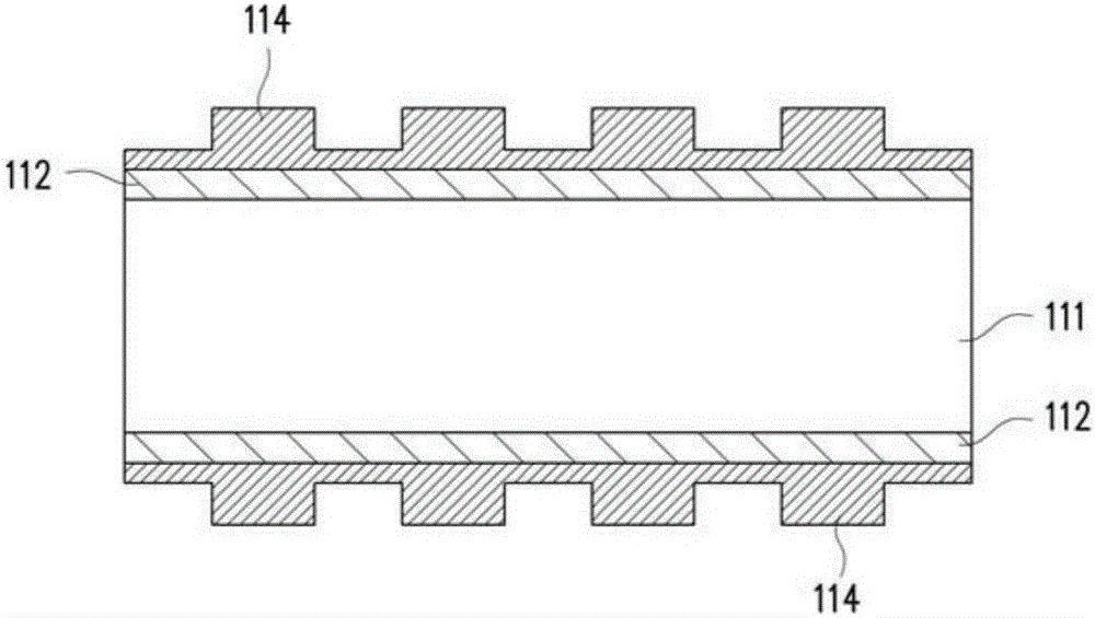
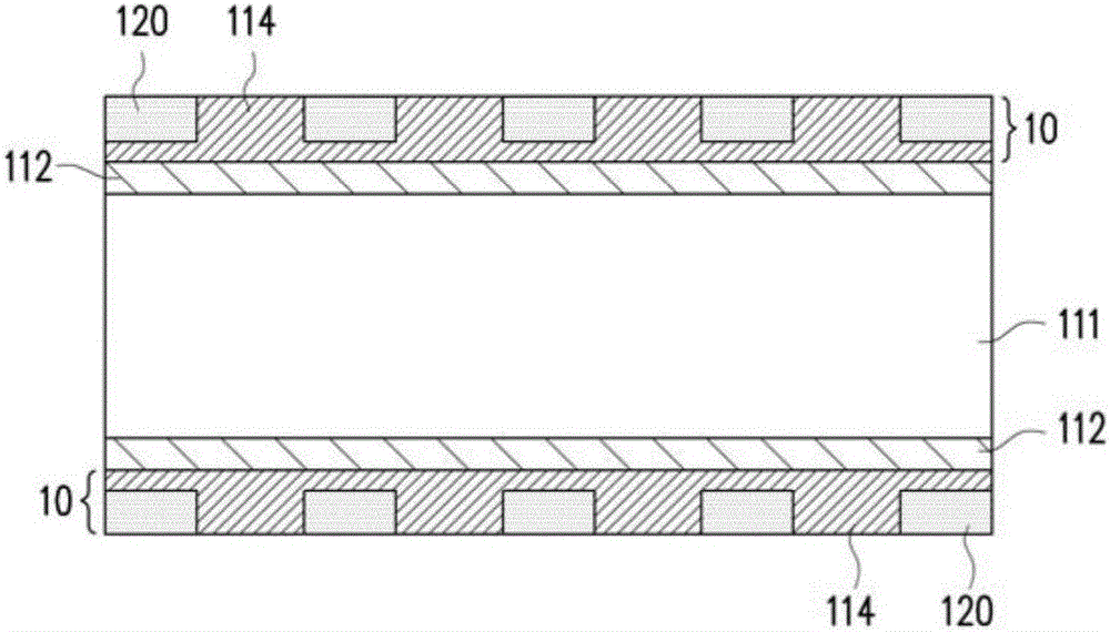
[0033] Figure 1A to Figure 1H It is a schematic cross-sectional view of the manufacturing process of the semiconductor package structure according to an embodiment of the present invention. First, please refer to Figure 1A , providing a packaging substrate 110 . The packaging substrate 110 includes a dielectric layer 111, a first metal layer 112 connected to the dielectric layer 111, and a second metal layer 113 connected to the first metal layer 112, wherein the first metal layer 112 is located between the dielectric layer 111 and the second metal layer Between 113. In this embodiment, the number of the first metal layer 112 and the number of the second metal layer 113 are two respectively. The aforementioned two first metal layers 112 are respectively located on opposite sides of the dielectric layer 111 , and each second metal layer 113 is connected to the corresponding first metal layer 112 . The material of the dielectric layer 111 can be silicon oxide, silicon nitri...


PUM


Abstract

The invention provides a semiconductor package structure and a manufacturing method thereof which comprises the following steps: a semiconductor package substrate is provided; the package substrate includes a dielectric layer, a first metal layer connecting the dielectric layer, and a second metal layer connecting the first metal layer; the first metal layer is located between the dielectric layer and the second metal layer; the second metal layer is patterned to form a line layer; a first encapsulant is formed on the line layer and a portion of the line layer is exposed; the dielectric layer and the first metal layer are removed; a chip is configured on the first encapsulant and electrically connected to the line layer exposed by the first encapsulant; a second encapsulant is formed on the first encapsulant and wraps the chip. The semiconductor package structure obtained by the method provided by the invention does not have a core layer, so that the semiconductor package structure can have a smaller thickness to meet the miniaturization development requirements.

Description

technical field [0001] The invention relates to a packaging structure and a manufacturing method thereof, in particular to a semiconductor packaging structure and a manufacturing method thereof. Background technique [0002] In the semiconductor industry, the production of integrated circuits (ICs) can be mainly divided into three stages: design of integrated circuits, fabrication of integrated circuits, and packaging of integrated circuits. After the integrated circuits of the wafer are fabricated, the active surface of the wafer is provided with a plurality of die pads. Finally, the bare chips obtained by dicing the wafer can be electrically connected to the carrier through the chip pads. Generally speaking, the carrier can be a lead frame or a package substrate, and the chip can be connected to the carrier by wire bonding or flip chip bonding to achieve The chip pads of the chip are electrically connected to the contacts of the carrier, thereby forming a chip package. ...

Claims


Application Information

Patent Timeline
Patent Type & Authority Applications(China)
IPC IPC(8): H01L21/56H01L23/31
CPCH01L21/56H01L23/3171
Inventor 陈宪章
Owner CHIPMOS TECH INC
Why Eureka
Try Eureka