Novel microstrip line packaging structure of substrate integrated gap waveguide

A technology of substrate integration and gap waveguide, applied in the field of electronics, can solve problems such as no public reports, achieve the effects of reducing space radiation, solving radiation loss and plane wave, and wide bandwidth

Inactive Publication Date: 2017-06-13
YUNNAN UNIV
View PDF3 Cites 8 Cited by
  • Summary
  • Abstract
  • Description
  • Claims
  • Application Information

AI Technical Summary

Problems solved by technology

[0006] Contents of the present invention, through literature search, do not see the public report identical with the present invention

Method used


Image

  • Novel microstrip line packaging structure of substrate integrated gap waveguide
  • Novel microstrip line packaging structure of substrate integrated gap waveguide
  • Novel microstrip line packaging structure of substrate integrated gap waveguide

Examples


Embodiment Construction

[0037] The technical solution of the present invention will be further described in detail below in combination with specific embodiments.

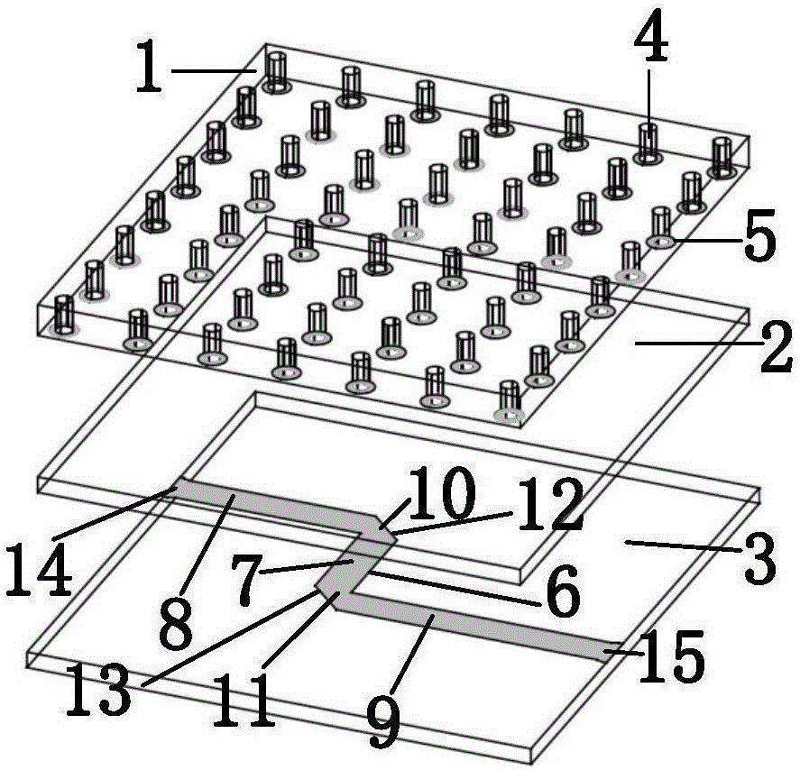
[0038] Such as Figure 1-6 As shown, a new substrate-integrated gap waveguide packaged microstrip line structure, including: a top dielectric board (1), a middle dielectric board (2), and a bottom dielectric board (3), wherein:

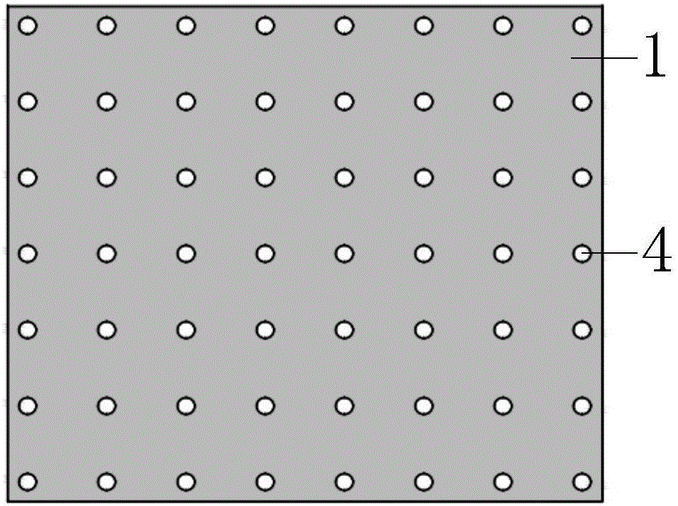
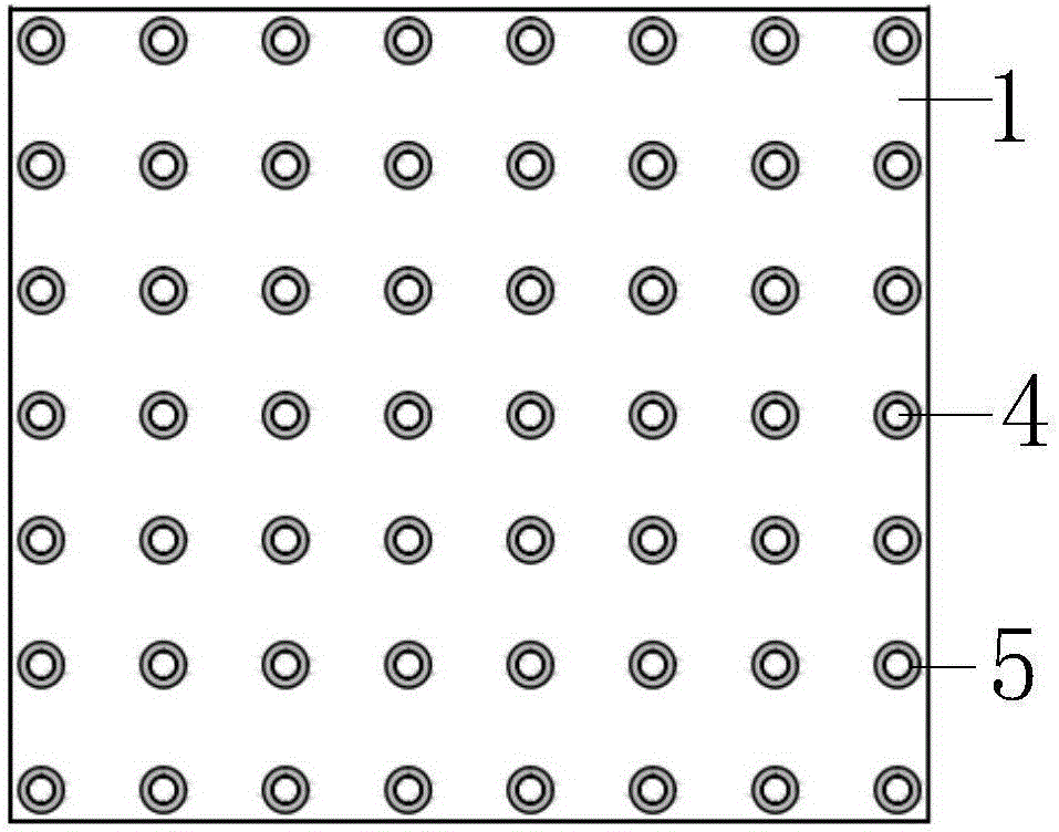
[0039] a. The upper surface of the top dielectric board (1) is printed with a metal layer, the dielectric board (1) is punched with periodic metal vias (4), and the lower surface of the dielectric board (1) is coated with periodic metal circular holes The patch (5), the periodic metal vias and the periodic metal circular patch (5) together form a mushroom-shaped electromagnetic bandgap (EBG) structure;

[0040] b. The middle dielectric board (2) is the gap layer, which is located in the middle of the top dielectric board (1) and the bottom dielectric board (3);

[0041] c. The upper surface of the bottom dielec...


PUM


Abstract

The invention relates to a novel microstrip line packaging structure of a substrate integrated gap waveguide. The microstrip line packaging structure is formed by three layers of medium plates in an adhesion mode, wherein the medium plates comprise the top layer medium plate (1), the middle layer medium plate (2) and the bottom layer medium plate (3). Periodical metal via holes (4) are formed in the top layer medium plate (1), a metal layer is printed on the upper surface of the top layer medium plate (1), and metallic wound patches (5) are applied to the lower surface of the top layer medium plate (1); chamfered bent microstrip lines (8, 9, 10 and 11) are arranged on the bottom layer medium plate (3), and a metal layer is printed on the lower surface of the bottom layer medium plate (3). A microstrip line is packaged, the problems that irradiation loss, plane waves and cavity resonance exist in a traditional microstrip line are solved, and meanwhile the novel microstrip line packaging structure has the advantages of being simple in structure, small in dimension, large in band width, low in loss, stable in structure and the like, and is easier to integrate and machine.

Description

technical field [0001] The invention relates to the field of electronic technology, in particular to a novel packaged microstrip line structure of substrate-integrated gap waveguide. Background technique [0002] Microstrip line is a kind of transmission line used to transmit microwave signals, and it has been widely used in many fields. Compared with metal waveguides, microstrip lines have the characteristics of small size, light weight, wide operating frequency band, high reliability and low manufacturing cost. Traditional microstrip lines suffer from radiation loss, plane waves, and cavity resonances. [0003] Stripline and substrate-integrated waveguides have good performance in suppressing space radiation, but the vertical asymmetry of stripline will generate harmful high-order modes. Since the substrate integrated waveguide (Substrate Integrated Waveguide, SIW) transmits TE 10 mode, when SIW is integrated with TEM / quasi-TEM mode microstrip lines, mode conversion los...

Claims


Application Information

Patent Timeline
Patent Type & Authority Applications(China)
IPC IPC(8): H01P3/08
CPCH01P3/082
Inventor 张秀普申东娅张晶董明王珂
Owner YUNNAN UNIV
Why Eureka
Try Eureka