High-transmittance metal grid flexible conductive film and preparation process thereof

A metal grid, flexible conductive technology, applied in the direction of cable/conductor manufacturing, conductive layer on the insulating carrier, circuit, etc., can solve the problems that are not very complete, difficult to balance conductivity and light transmittance, etc.

Active Publication Date: 2017-06-16
SHANGHAI JIAO TONG UNIV
View PDF5 Cites 13 Cited by
  • Summary
  • Abstract
  • Description
  • Claims
  • Application Information

AI Technical Summary

Problems solved by technology

However, the existing technology is not very complete, especially it is difficult to balance the two properties of conductivity and light transmittance
Also, uniformity is a big technical challenge

Method used


Image

  • High-transmittance metal grid flexible conductive film and preparation process thereof
  • High-transmittance metal grid flexible conductive film and preparation process thereof
  • High-transmittance metal grid flexible conductive film and preparation process thereof

Examples


Embodiment 1

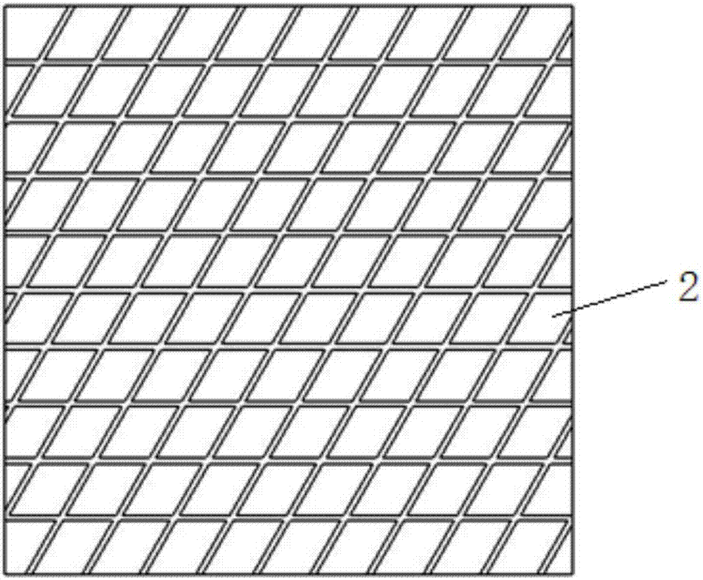
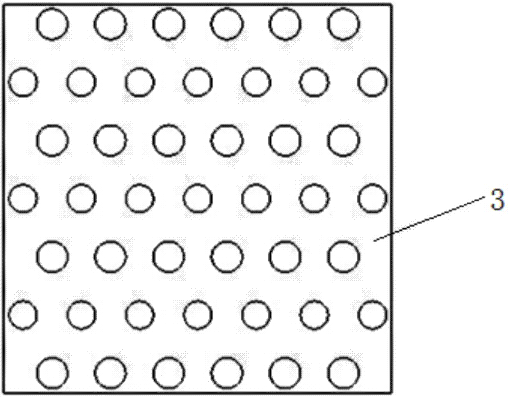
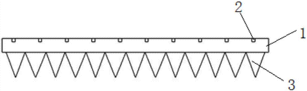
[0032] Such as Figure 1~3 As shown, a metal grid flexible conductive film with high light transmittance includes a flexible base layer 1, a metal grid layer 2 on one side, and a UV-cured nanostructure layer 3 on the other side. The metal grid layer 2 plays the role of conduction, and the UV-cured nanostructure layer 3 plays the role of increasing light transmittance.

[0033] The flexible base layer 1 is a transparent, bendable polymer material, including common PET, PEN, PI, PPS, PC, PES, PEI, PAR or PCO flexible polymer materials.

[0034] The metal grid layer 2 is a conductive grid layer obtained by rolling linear intersecting grooves on the surface of the flexible base layer, then coating silver paste into the linear intersecting grooves, baking and cleaning.

[0035] The UV-curable nanostructure layer 3 is a transparent glue with UV-curable function, which is formed by UV-curing after embossing on the flexible base layer to form a nanostructure array with improved light...

Embodiment 2

[0048] A metal grid flexible conductive film with high light transmittance comprises a flexible base layer, a metal grid layer on one side and a UV curable nanostructure layer on the other side. The metal grid layer plays the role of conduction, and the UV-cured nanostructure layer plays the role of increasing light transmittance.

[0049] The flexible base layer is PET.

[0050] The metal grid layer is a conductive grid layer obtained by rolling linear intersecting grooves on the surface of the flexible base layer, then coating silver paste into the linear intersecting grooves, baking and cleaning. The linear intersecting grooves are composed of two groups of parallel linear grooves intersecting at an angle of 10°, wherein the groove width of each linear groove is 50nm, and the distance between adjacent linear grooves is 100nm.

[0051] The UV-curable nanostructure layer is a transparent glue with UV-curable function, which is formed by UV-curing after embossing on the flexi...

Embodiment 3

[0053] A metal grid flexible conductive film with high light transmittance comprises a flexible base layer, a metal grid layer on one side and a UV curable nanostructure layer on the other side. The metal grid layer plays the role of conduction, and the UV-cured nanostructure layer plays the role of increasing light transmittance.

[0054] The flexible base layer is PCO flexible polymer material.

[0055] The metal grid layer is a conductive grid layer obtained by rolling linear intersecting grooves on the surface of the flexible base layer, then coating silver paste into the linear intersecting grooves, baking and cleaning. The linear intersecting grooves are composed of two groups of parallel linear grooves intersecting at an angle of 90°, wherein the groove width of each linear groove is 10 μm, and the distance between adjacent linear grooves is 500 μm.

[0056] The UV-curable nanostructure layer is a transparent glue with UV-curable function, which is formed by UV-curing ...


PUM

PropertyMeasurementUnit
widthaaaaaaaaaa
widthaaaaaaaaaa
diameteraaaaaaaaaa

Abstract

The invention relates to a high-transmittance metal grid flexible conductive film and a preparation process thereof. The high-transmittance metal grid flexible conductive film comprises a flexible substrate layer, a metal grid layer arranged at one side of the flexible substrate layer, and an UV curing nano structure layer arranged at the other side. The preparation process specifically comprises the steps of impressing metal grid straight-line grooves through an R2R process at one side of a flexible substrate; then performing silver paste scrape coating and solidification in the metal grid straight-line grooves so as to acquire a metal grid layer; and then performing impressing and curing by adopting an UV curing process so as to perform a nano structure with high transmittance at the other side of the flexible substrate layer. The process method provided by the invention further improves the transmittance of a transparent conductive film because of existence of the anti-reflection nano structure compared with an existing metal grid flexible conductive film. Meanwhile, the R2R processing method is adopted, so that the efficiency is greatly improved, and large-scale production is facilitated. Products prepared according to the method have wide application prospects in the fields such as flexible electronics and touch screens.

Description

technical field [0001] The invention relates to a flexible electronic technology, in particular to a flexible conductive film with high light transmittance and a preparation process thereof. Background technique [0002] Due to the shortcomings of traditional rigid electronic devices such as poor ductility, insufficient bending resistance, and heavy weight, more and more engineering applications and demands call for the birth of flexible electronic devices. Flexible electronic devices Fabricate organic / inorganic electronic devices on flexible polymer films, plastic or thin metal substrates, so that the prepared devices have both flexibility and electronic composite functions. Since the technology was proposed, it has attracted more and more researchers to continuously explore and make breakthroughs. Due to the advantages of high-efficiency production and low-cost manufacturing, this technology has broad application prospects in information, energy, medical, national defense...

Claims


Application Information

Patent Timeline
Patent Type & Authority Applications(China)
IPC IPC(8): H01B5/14H01B13/00
CPCH01B5/14H01B13/00
Inventor 易培云张成鹏张伟鑫彭林法来新民
Owner SHANGHAI JIAO TONG UNIV
Why Eureka
Try Eureka