High holding current ldmos structure for high voltage esd protection

An ESD protection and high-maintenance technology, which is applied in the field of electronic science and technology, can solve problems such as the threat of sophisticated integrated circuits and LDMOS damage, and achieve the effects of avoiding latch-up effects, improving robustness, and increasing sustaining current

Active Publication Date: 2019-12-06
UNIV OF ELECTRONICS SCI & TECH OF CHINA
View PDF4 Cites 0 Cited by
  • Summary
  • Abstract
  • Description
  • Claims
  • Application Information

AI Technical Summary

Problems solved by technology

But it is such a common electrical phenomenon that is a fatal threat to sophisticated integrated circuits.
[0003] For high-voltage integrated circuits, due to the existence of similar latch-up effects, the LDMOS structure ( figure 1 shown) usually cannot be directly used in the
However, if the maintenance voltage of LDMOS is increased to above the VDD voltage by some methods, although it can bring latch-up immunity, it will also increase the voltage that the device can withstand in the on state, coupled with the influence of the Kerke effect under high current, LDMOS will quickly produce irreversible damage

Method used


Image

  • High holding current ldmos structure for high voltage esd protection
  • High holding current ldmos structure for high voltage esd protection
  • High holding current ldmos structure for high voltage esd protection

Examples


Embodiment 1

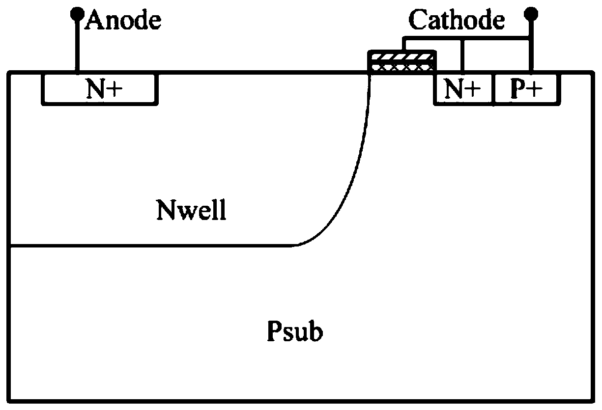
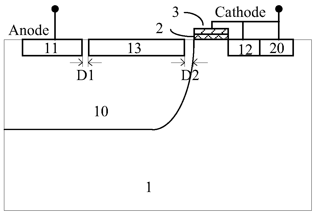
[0026] Such as figure 2 As shown, a high sustaining current LDMOS structure for high-voltage ESD protection includes a P-type substrate 1, an NWELL region 10 located on the surface of the P-type substrate, an NPLUS contact region 11 located inside the NWELL region, and the right side of the NWELL region 10 The thin gate oxide layer 2 on the surface of the P-type substrate whose side is tangential, the polysilicon gate electrode 3 located above the thin gate oxide layer 2, and the NPLUS source contact implanted on the P-substrate surface tangential to the right side of the thin gate oxide layer 2 Region 12, the PPLUS substrate 20 tangent to the right side of the NPLUS source contact region 12, the NTOP layer 13 located on the right side of the NPLUS contact region 11 inside the NWELL region 10, the distance between the left edge of the NTOP layer 13 and the right edge of the NPLUS contact region 11 D1, the distance between the right edge of the NTOP layer 13 and the right edge...

Embodiment 2

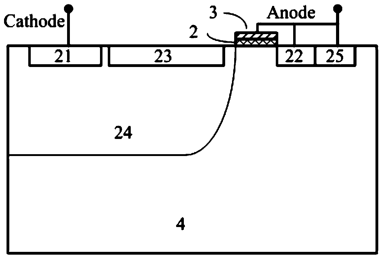
[0037] Such as image 3 As shown, a high sustaining current LDMOS structure for high-voltage ESD protection is different from Embodiment 1 in that: the NPLUS contact region 11 is replaced by the first PPLUS injection region 21, and the NPLUS source contact region 12 is replaced by The second PPLUS injection region 22, the NTOP layer 13 is replaced by a PTOP layer 23, the PPLUS substrate 20 is replaced by a substrate contact NPLUS region 25, the NWELL region 10 is replaced by a PWELL region 24, and the P-type substrate 1 is replaced by an N-type substrate 4, the first PPLUS implantation region 21 constitutes the cathode contact of the device, and the second PPLUS implantation region 22, the substrate contact NPLUS region 25, and the polysilicon gate electrode 3 are short-circuited to constitute the anode contact of the device.

[0038] The working principle of this embodiment is basically the same as that of Embodiment 1, the difference is that this embodiment additionally uses...


PUM


Abstract

The invention provides a high sustaining current LDMOS structure for high-voltage ESD protection, including a P-type substrate, an NWELL region, an NP contact region, a thin gate oxide layer on the surface of the P-type substrate, a polysilicon gate electrode, and implantation on the surface of the P-type substrate. The NP source contact area, PP substrate, NTOP layer, the distance between the left edge of the NTOP layer and the right edge of the NP contact area is D1, the distance between the right edge of the NTOP layer and the right edge of the NWELL area is D2, and the device can be adjusted by adjusting D1 To maintain the current, adjust the trigger voltage of the device by adjusting D2. The present invention proposes that the LDMOS device can adjust the trigger voltage through the position of the NTOP layer without changing the process; the change of the position of the NTOP layer can adjust the trigger voltage on the one hand, and the other On the one hand, the holding current can be increased to avoid the latch-up effect; the existence of the NTOP layer can change the current distribution and improve the robustness of the device under the ESD pulse current.

Description

technical field [0001] The invention belongs to the field of electronic science and technology, and is mainly used for the protection technology of Electro Static Discharge (ESD for short), and specifically relates to a high sustaining current LDMOS structure for high-voltage ESD protection. Background technique [0002] ESD stands for Electrostatic Discharge, which is a common phenomenon in nature. ESD exists in every corner of people's daily life. But it is such a common electrical phenomenon that is a fatal threat to sophisticated integrated circuits. [0003] For high-voltage integrated circuits, due to the existence of similar latch-up effects, the LDMOS structure ( figure 1 shown) usually cannot be directly used in it. However, if the maintenance voltage of LDMOS is increased to above the VDD voltage by some methods, although it can bring latch-up immunity, it will also increase the voltage that the device can withstand in the on state, coupled with the influence of...

Claims


Application Information

Patent Timeline
Patent Type & Authority Patents(China)
IPC IPC(8): H01L29/78
CPCH01L29/7816
Inventor 乔明齐钊杨文张波
Owner UNIV OF ELECTRONICS SCI & TECH OF CHINA
Why Eureka
Try Eureka