

Packaging structure of OLED device and preparation method for packaging structure, and metal mask plate
A packaging structure and device technology, applied in the field of OLED devices, can solve the problems of OLED device falling off and the influence of bending performance of OLED devices, and achieve the effect of improving bending performance and reducing bending stress
- Summary
- Abstract
- Description
- Claims
- Application Information
AI Technical Summary
Problems solved by technology
Method used
Image

Examples
Embodiment Construction
[0033] In order to enable those skilled in the art to better understand the technical solutions of the present invention, the encapsulation structure of an OLED device and its preparation method and metal mask provided by the present invention will be described in further detail with reference to the accompanying drawings and specific embodiments. . In the drawings, the same reference numerals are used throughout the specification and the drawings to denote the same structures and regions.
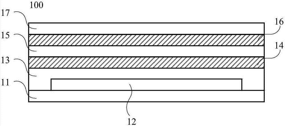
[0034] See figure 1 , figure 1 It is a schematic structural diagram of the packaging structure of an OLED device in the prior art. Such as figure 1 As shown, the OLED device 12 is prepared on a transparent flexible substrate 11, and the encapsulation structure 100 of the OLED device 12 is alternately formed on the OLED device 12 with barrier layers 13, 15, 17 and buffer layers 14, 16 covering each other. Among them, the barrier layers 13, 15, 17 are used to effectively block water and oxygen...
PUM
 Abstract
Description
Claims
Application Information