Copper clad ceramic substrate facilitating laser cutting

A copper-clad ceramic substrate and laser cutting technology, which is applied in the direction of semiconductor/solid-state device parts, semiconductor devices, electrical components, etc., can solve the problems of difficulty in breaking the process and achieve the effect of preventing air leakage.

Active Publication Date: 2017-06-27
江苏富乐华半导体科技股份有限公司
View PDF3 Cites 4 Cited by
  • Summary
  • Abstract
  • Description
  • Claims
  • Application Information

AI Technical Summary

Problems solved by technology

The copper-clad ceramic substrate structure of the present invention can increase the suction pressure, achieve uniform surface height of the DBC substrate during cutting, controllable cutting depth, and improve product yield; the connection of the process edge is designed with thin copper wires, which can effectively solve the problem of process edge Difficult edge breaking after connection

Method used


Image

  • Copper clad ceramic substrate facilitating laser cutting
  • Copper clad ceramic substrate facilitating laser cutting
  • Copper clad ceramic substrate facilitating laser cutting

Examples


Embodiment 1

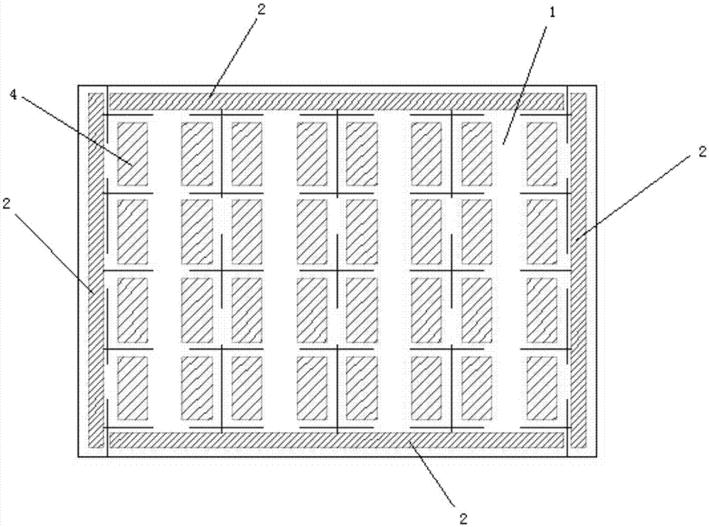
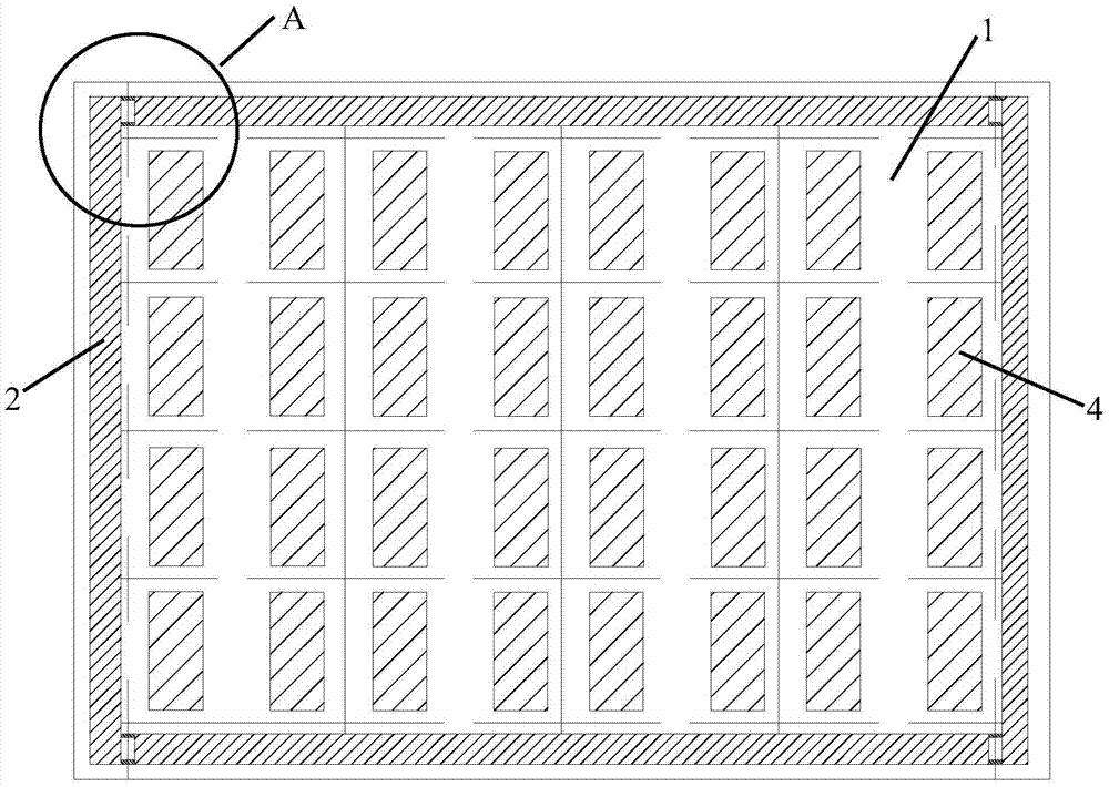
[0022] Such as Figure 2-3 A copper-clad ceramic substrate that is convenient for laser cutting is shown, comprising: a copper-clad ceramic substrate body 1 , a process side 2 and a copper strip 3 .

[0023] The copper-clad ceramic substrate body 1 has a rectangular structure.

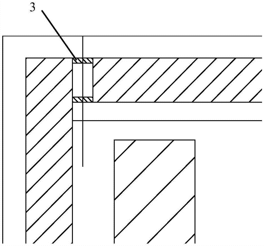
[0024] The process side 2 is arranged around the edge of the copper-clad ceramic substrate body 1, and consists of four straight sides: upper, lower, left, and right; two mutually perpendicular process sides 2 are connected by copper strips 3 to form a connection unit, and the copper strips The width of 3 is smaller than the width of process side 2. The width of the process side is 5mm.

[0025] The number of copper strips in the connection unit is two (the width of each copper strip is 0.5mm), and the two copper strips extend from the two sides of the edge of one of the process sides to the other process side along the straight line where the process side is located, so that Connect two process edg...


PUM

PropertyMeasurementUnit
Widthaaaaaaaaaa
Widthaaaaaaaaaa

Abstract

The invention relates to the design field for cutting of a copper clad ceramic substrate and discloses a copper clad ceramic substrate facilitating laser cutting. The copper clad ceramic substrate facilitating laser cutting is characterized by comprising a copper clad ceramic substrate body, process edges and copper bars, wherein the copper clad ceramic substrate body has a rectangular structure; the process edges are arranged around the edges of the copper clad ceramic substrate body and are composed of an upper straight edge, a lower straight edge, a left straight edge and a right straight edge; and two mutually-vertical process edges are connected by the copper bar to form a connection unit, and the width of the copper bar is smaller than the width of the process edge. According to the copper clad ceramic substrate structure of the invention, the suction pressure can be improved, high uniformity of the surface of the DBC substrate in the case of cutting can be realized, the cutting depth is controllable, and the product yield is improved; and as the process edge connection place adopts a thin copper wire design, the problem of difficult edge snapping after the process edges are connected can be effectively solved.

Description

technical field [0001] The invention belongs to the field of cutting design of copper-clad ceramic substrates, in particular to a copper-clad ceramic substrate which is convenient for laser cutting. Background technique [0002] Copper-clad ceramic substrate (DBC substrate) is an electronic basic material made by directly sintering copper foil on the ceramic surface using DBC (Direct Bond Copper) technology. The copper-clad ceramic substrate has excellent thermal cycle performance, stable shape, good rigidity, high thermal conductivity, and high reliability. The copper-clad surface can be etched with various graphics, and it is a pollution-free and pollution-free Green products, the use temperature is quite wide, can be from -55 ° C to 850 ° C, the thermal expansion coefficient is close to silicon, and its application fields are very wide: it can be used in semiconductor refrigerators, electronic heaters, high-power power semiconductor modules, power control circuits, Power...

Claims


Application Information

Patent Timeline
IPC IPC(8): H01L23/15
CPCH01L23/15
Inventor 管鹏飞贺贤汉李德善
Owner 江苏富乐华半导体科技股份有限公司
Why Eureka
Try Eureka