

Thin-film transistor, method for manufacturing same, array substrate and display device
A technology of thin film transistors and array substrates, which is applied in the display field, can solve the problems of poor stability of amorphous silicon TFTs and poor ohmic contact of amorphous silicon TFTs, and achieve improved contact effects, improved working stability, and increased contact areas. Effect
Active Publication Date: 2017-06-27
BOE TECH GRP CO LTD
View PDF2 Cites 0 Cited by
- Summary
- Abstract
- Description
- Claims
- Application Information
AI Technical Summary
Problems solved by technology
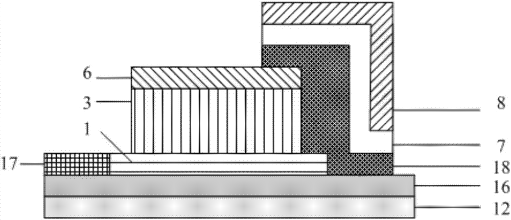
Although figure 1 The vertical TFT structure shown can greatly reduce the size of the TFT, but the vertical TFT structure is only applicable to the oxide TFT at present, and the amorphous silicon is used as the active layer in the amorphous silicon TFT, because the active layer and the source The electrode metal layer and the drain metal layer are in direct contact, so the ohmic contact of the amorphous silicon TFT is poor, resulting in poor stability of the amorphous silicon TFT
Method used
View moreImage
Smart ImageViewing Examples

Examples
preparation example Construction
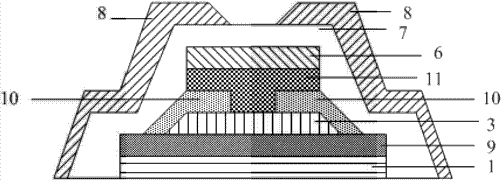
[0048] Corresponding to the thin film transistor provided in the embodiment of the present application, the embodiment of the present application also provides a thin film transistor manufacturing method, such as Figure 5 As shown, the method includes:
[0049] S501, setting a first ohmic contact layer on the source metal layer;
[0050] S502, disposing a first insulating layer on the first ohmic contact layer;
[0051] S503, disposing an active layer in contact with the first ohmic contact layer on the first insulating layer;
[0052] S504, setting a second ohmic contact layer on the active layer.
Login to View More PUM
 Abstract
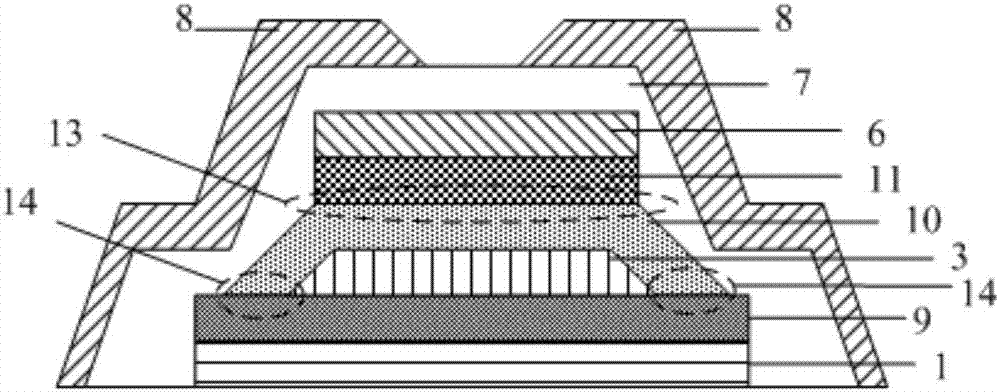
The invention discloses a thin-film transistor, a method for manufacturing the same, an array substrate and a display device. An active layer is not in direct contact with the source metal layer and the drain metal layer in the thin-film transistor, thereby reducing the ohmic contact resistance between the active layer and the source metal layer and between the active layer and the drain metal layer, improving an ohmic contact effect between the active layer and the source metal layer and between the active layer and the drain metal layer in the vertical amorphous silicon thin-film transistor, and further improving the operating stability of the thin-film transistor. The embodiment of the invention provides a thin-film transistor comprising the source metal layer, a first ohmic contact layer on the top of the source metal layer, a first insulating layer on the top of the first ohmic contact layer, the active layer on the top of the first insulating layer and in contact with the first ohmic contact layer, a second ohmic contact layer on the top of the active layer; and the drain metal layer on the top of the second ohmic contact layer.
Description
technical field [0001] The present application relates to the field of display technology, in particular to a thin film transistor and a manufacturing method thereof, an array substrate, and a display device. Background technique [0002] At present, high-resolution display products have become the mainstream trend in the market. To achieve high-resolution display of liquid crystal display panels, the requirements for pixel aperture ratio are getting higher and higher. Therefore, reducing the size of thin film transistors (Thin Film Transistor, TFT) has become particularly critical. . In the prior art, there is a vertical TFT structure, which can greatly reduce the size of the TFT, such as figure 1 As shown, the vertical TFT structure includes: a glass substrate 12, a buffer layer 16, a pixel layer 17, a source metal layer 1, a first insulating layer 3, an oxide (IGZO) layer 18, a drain metal layer 6, a second The insulating layer 7 and the gate metal layer 8, wherein the ...
Claims
Login to View More Application Information
Patent Timeline
 Patent Type & AuthorityApplications(China)
IPC IPC(8): H01L29/786H01L21/336H01L27/12
CPCH01L27/124H01L29/66742H01L29/786H01L29/78639
Inventor张慧林允植严允晟
OwnerBOE TECH GRP CO LTD