Acousto-optic crystal and transducer bonding structure

A technology of transducers and crystals, applied in the fields of instruments, optics, nonlinear optics, etc., can solve the problems of device failure and scrap, shorten the life of the device, and reduce the aggregation density of the film layer, so as to reduce the thermal stress of the device and keep the device performance stable. Effect

Active Publication Date: 2019-09-13
CHINA ELECTRONICS TECH GRP NO 26 RES INST
View PDF5 Cites 0 Cited by
  • Summary
  • Abstract
  • Description
  • Claims
  • Application Information

AI Technical Summary

Problems solved by technology

[0006] ③After the device undergoes a thermal cycle, the cracking and adhesion problems of the transducer will deteriorate, and even the transducer will automatically fall off along the cracking direction, seriously affecting the performance of the device, or causing the device to fail and be scrapped
[0010] None of the above measures can solve the problem well
Scheme ① will lead to a decrease in the aggregation density of the film layer and affect the quality of the film layer. Scheme ② needs to greatly extend the production cycle of the device, and the improvement effect on the bonding effect is not obvious. In addition, the aging treatment may shorten the life of the device

Method used


Image

  • Acousto-optic crystal and transducer bonding structure
  • Acousto-optic crystal and transducer bonding structure
  • Acousto-optic crystal and transducer bonding structure

Examples


Embodiment Construction

[0028] The present invention will be described in detail below in conjunction with the accompanying drawings and specific embodiments.

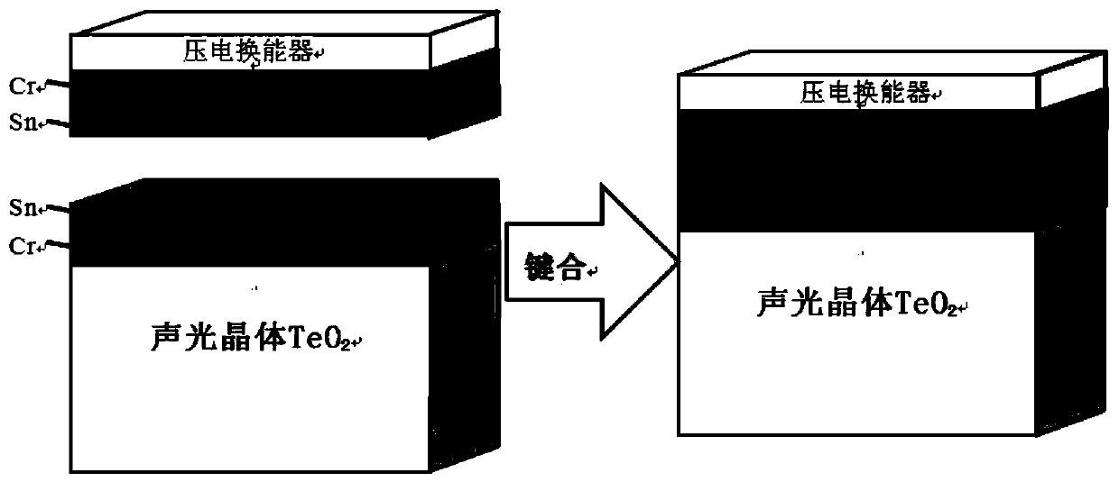
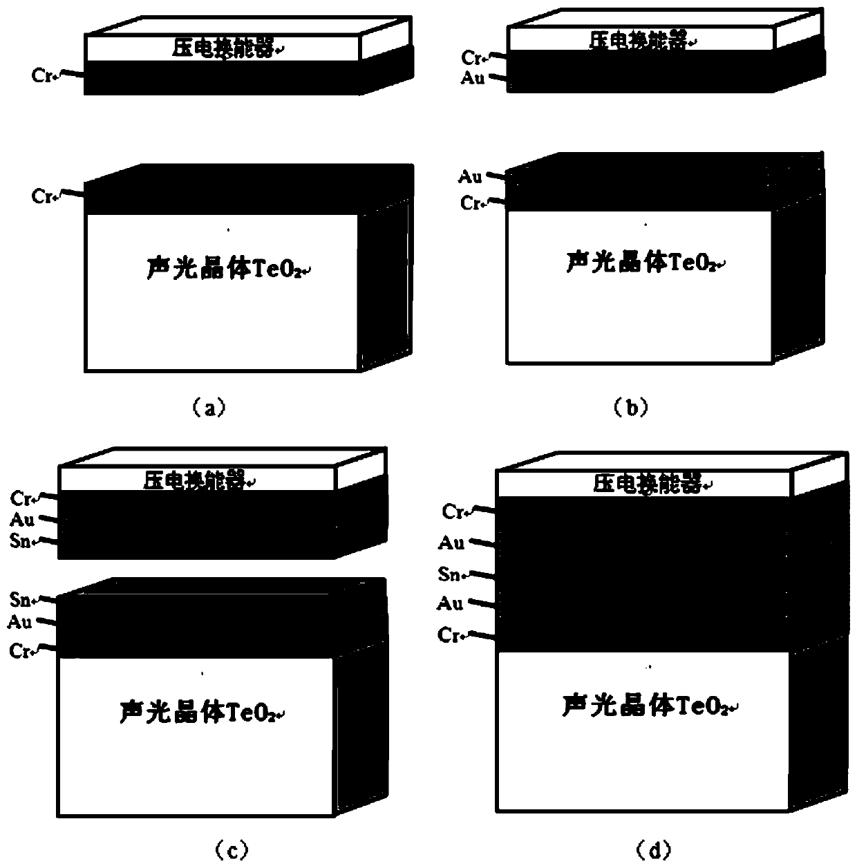
[0029] In order to ensure device reliability and environmental adaptability, the present invention adds a metal transition layer between the acousto-optic crystal and the bottom electrode (Cr) of the transducer and the welding layer. The metal transition layer meets the following requirements: ①High electrical conductivity and good electrical conductivity; ②Good adhesion between the bottom electrode layer Cr and the solder layer Sn; ③The addition of the metal transition layer effectively reduces the thermal stress at the interface between the crystal and the bottom electrode; ④Under the conditions of the first three items are met, the loss of the transducer will not be increased, and the bonding layer meets the acoustic impedance matching. Based on the above considerations, the material of the transition layer is Au (which can satisfy the fir...


PUM

PropertyMeasurementUnit
thicknessaaaaaaaaaa
thicknessaaaaaaaaaa
thicknessaaaaaaaaaa

Abstract

The invention discloses an acoustooptic crystal and transducer bonding structure. A bottom electrode layer and a welding layer are sequentially plated on the surface of each of an acoustooptic crystal and a transducer; the welding layer of the acoustooptic crystal is bonded with the welding layer of the transducer together; metal transition layers are arranged between the bottom electrode layer and the welding layer of the acoustooptic crystal as well as between the bottom electrode layer and the welding layer of the transducer respectively; after each welding layer is adhered to the corresponding bottom electrode layer through the corresponding metal transition layer, the adhesive force between the bottom electrode layer and the acoustooptic crystal is larger than that between the bottom electrode layer and the acoustooptic crystal when the welding layer is directly adhered to the corresponding bottom electrode layer; and the thickness of each metal transition layer enables a bonding layer to meet the acoustic impedance matching requirement of a device wholly. As for the acoustooptic crystal and transducer bonding structure, after bonding, the surface of the transducer does not have the phenomenon of cracking any more, the strength and the adhesive force of the transducer are strengthened, and the thermal stress of the device is obviously lowered.

Description

technical field [0001] The invention relates to a bonding structure in the processing of an acousto-optic device, which is used to solve problems such as transducer cracking and falling off after bonding, thereby improving the environmental adaptability and reliability of the device, and belongs to the technical field of acousto-optic devices. Background technique [0002] Acousto-optic crystals (TeO 2 Mainly) and the piezoelectric transducer are bonded together through the diffusion of metal atoms by a bonding process. Several metal film layers need to be plated between the crystal and the transducer, collectively referred to as the bonding layer. Commonly used acousto-optic device bonding layer structure and bonding process such as figure 1 shown. First, the bonding layer is plated on the surface of the crystal and the transducer respectively. The bonding layer is composed of a bottom electrode layer and a welding layer. The material of the bottom electrode layer is usu...

Claims


Application Information

Patent Timeline
Patent Type & Authority Patents(China)
IPC IPC(8): G02F1/11
Inventor 陆川刘伟陈华志米佳张永川
Owner CHINA ELECTRONICS TECH GRP NO 26 RES INST
Why Eureka
Try Eureka