A kind of semiconductor device and its manufacturing method

A manufacturing method, semiconductor technology, applied in semiconductor/solid-state device manufacturing, semiconductor devices, electric solid-state devices, etc., can solve problems such as fin top damage, fin damage, narrow fin damage, etc., and achieve high carrier migration Efficiency, improved performance, avoiding damage problems

Active Publication Date: 2019-12-17
SEMICON MFG INT (SHANGHAI) CORP +1
View PDF3 Cites 0 Cited by
  • Summary
  • Abstract
  • Description
  • Claims
  • Application Information

AI Technical Summary

Problems solved by technology

However, such a large dose of doping leads to serious damage to the narrow fins, and it is difficult to repair the damage to the fins even with the annealing treatment after ion implantation, and the damaged fins significantly reduce the carrier mobility and De-activation of doping impurities
[0005] In addition, the currently commonly used process is that deep well isolation implantation is performed before fin formation, and Anti-Punch Trough (APT) ion implantation is performed after fin formation. Anti-body breakdown ion implantation is beneficial to control the loss of doping impurities, but a large number of implanted ions can also cause damage to the fins. There are a large number of damage points on the fins. It is found that the damage is especially serious on the top of the fins.

Method used


Image

  • A kind of semiconductor device and its manufacturing method
  • A kind of semiconductor device and its manufacturing method
  • A kind of semiconductor device and its manufacturing method

Examples


Embodiment 1

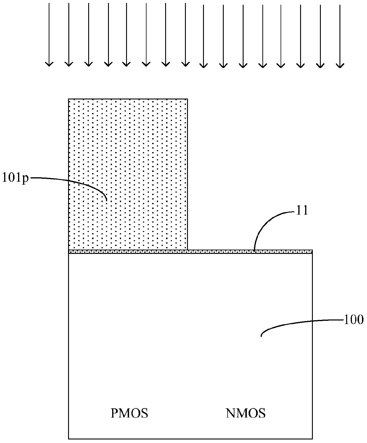
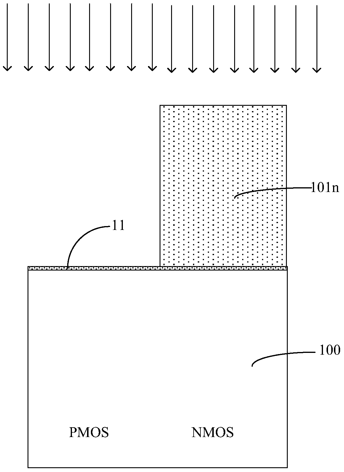
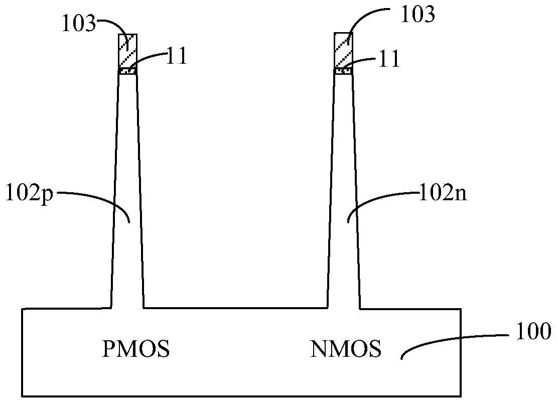
[0068] Below, refer to Figures 1A to 1O and figure 2 To describe a method for manufacturing a semiconductor device provided by an embodiment of the present invention. of which, 1A to Figure 1O A cross-sectional view of a structure formed by related steps of a method for manufacturing a semiconductor device according to an embodiment of the present invention; figure 2 It is a schematic flow chart of a method for manufacturing a semiconductor device according to an embodiment of the present invention.

[0069] Exemplarily, a method for manufacturing a semiconductor device according to an embodiment of the present invention includes the following steps:

[0070] First, step S201 is performed to provide a semiconductor substrate 100, the semiconductor substrate 100 includes a first region and a second region, and a first fin 102n is formed on the surface of the semiconductor substrate 100 corresponding to the first region , a second fin 102p is formed on the surface of the ...

Embodiment 2

[0129] The present invention also provides a manufacturing method of a semiconductor device. For details, refer to 3A to 3M and Figure 4 ,in, 3A to 3M and Figure 4 A cross-sectional view of a structure formed by related steps of a method for manufacturing a semiconductor device according to an embodiment of the present invention; Figure 4 It is a schematic flow chart of a method for manufacturing a semiconductor device according to another embodiment of the present invention.

[0130] Exemplarily, a method for manufacturing a semiconductor device according to an embodiment of the present invention includes the following steps:

[0131] First, step S401 is performed to provide a semiconductor substrate 300, the semiconductor substrate 300 includes a first region and a second region, and a first fin 302n is formed on the surface of the semiconductor substrate 300 corresponding to the first region , a second fin 302p is formed on the surface of the semiconductor substrat...

Embodiment 3

[0181] This embodiment also provides a semiconductor device obtained by using the manufacturing method in Embodiment 1, or a semiconductor device obtained by using the manufacturing method in Embodiment 2, and the semiconductor device may be a FinFET device.

[0182] The following reference Figure 3M The semiconductor device of the present invention will be described in detail.

[0183] The semiconductor device of the present invention includes: a semiconductor substrate 300, the semiconductor substrate 300 includes a first region and a second region, and a first well of a second conductivity type is formed in the semiconductor substrate corresponding to the first region , a second well of the first conductivity type is formed in the semiconductor substrate corresponding to the second region, a first fin 302n is formed on the surface of the semiconductor substrate corresponding to the first region, and A second fin 302p is formed on the surface of the semiconductor substrate...


PUM

PropertyMeasurementUnit
thicknessaaaaaaaaaa
thicknessaaaaaaaaaa
thicknessaaaaaaaaaa

Abstract

The invention provides a semiconductor device and a manufacturing method thereof. The manufacturing method comprises forming a first fin and a second fin on the surface of a semiconductor substrate; forming a first epitaxial layer doped with first-conduction-type doped impurity and a first liner layer sequentially on the surface of the semiconductor substrate, and exposed surfaces of the first fin and the second fin; removing the first liner layer and the first epitaxial layer in a first area; forming a second epitaxial layer doped with second-conduction-type doped impurity and a cover cap layer sequentially on the surface of the semiconductor substrate corresponding to the first area, and the exposed surface of the first fin; forming a sacrificial layer on the surface of the semiconductor substrate; removing the cover cap layer, the second epitaxial layer, the first liner layer and the first epitaxial layer on the sacrificial layer; removing the sacrificial layer, carrying out an annealing process, and removing the first liner layer and the cover cap layer; and forming a shallow trench shallow tunnel isolation structure on the surface of the semiconductor substrate. According to the invention, damage to the fins caused by ion implantation is avoided, and the performance of the semiconductor device is improved.

Description

technical field [0001] The present invention relates to the technical field of semiconductors, and in particular, to a semiconductor device and a manufacturing method thereof. Background technique [0002] With the continuous development of semiconductor technology, in order to improve the performance of the device, it is necessary to continuously reduce the size of the integrated circuit device. Compared with the existing planar transistors, the FinFET device has more superior performance in channel control and reduction of short-channel effects; the planar gate structure is arranged above the channel, and in the FinFET the gate It is arranged around the fins, so static electricity can be controlled from three sides, and the performance in static electricity control is also more prominent. [0003] There are many methods in the prior art for improving the performance of semiconductor devices, such as forming a super steep retrograde well (Super Steep Retrograde Well, SSRW ...

Claims


Application Information

Patent Timeline
Patent Type & Authority Patents(China)
IPC IPC(8): H01L21/8238H01L27/092
CPCH01L21/823431H01L27/0924H01L21/823821H01L29/66803
Inventor 李勇洪中山
Owner SEMICON MFG INT (SHANGHAI) CORP
Why Eureka
Try Eureka