Photo-stimulation and signal acquisition probe

A technology of signal acquisition and light stimulation, which is applied in light therapy, optical sensors, diagnosis with light, etc. It can solve the problems of inability to obtain neuronal feedback signals and limited optogenetics research functions, and achieve the effect of convenient operation

Inactive Publication Date: 2017-07-04
INST OF SEMICONDUCTORS - CHINESE ACAD OF SCI
View PDF5 Cites 7 Cited by
  • Summary
  • Abstract
  • Description
  • Claims
  • Application Information

AI Technical Summary

Problems solved by technology

[0003] At present, the existing experimental devices are not enough to meet the technical requirements of optogenetics research. A micro-LED neural probe in the prior art includes an LED drive unit and an LED light-emitting unit. This type of probe only has the function of photostimulation. The research function of optogenetics is limited, and the feedback signal generated by neurons under light stimulation cannot be obtained, and more in-depth research on optogenetics

Method used


Image

  • Photo-stimulation and signal acquisition probe
  • Photo-stimulation and signal acquisition probe
  • Photo-stimulation and signal acquisition probe

Examples


Embodiment 1

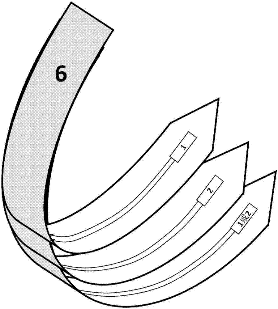
[0038] Such as figure 1 A miniature photo-stimulation and signal acquisition probe shown includes a probe substrate 6, the front end of the probe substrate 6 is sharp and sharp, and a light source 1 is integrated at the sharp end. This embodiment is an LED and a signal acquisition sensor 2 , the other end of the probe substrate is a metal contact electrode 3, 4, 5, through which the probe substrate can be connected with the external circuit, the light source 1, the sensor 2 and the electrode at both ends of the probe substrate 3, 4, and 5 are connected by metal wiring. The common electrode 4 is the common ground of the light source 1 and the sensor r2, the light source electrode 3 is the control signal and power supply line of the LED1, and the sensor electrode 5 is the signal collection and power supply line of the sensor 2.

[0039] The probe substrate 6 is a rigid rigid substrate. Among them, the material used for the rigid hard substrate is the common material of PCB, wh...

Embodiment 2

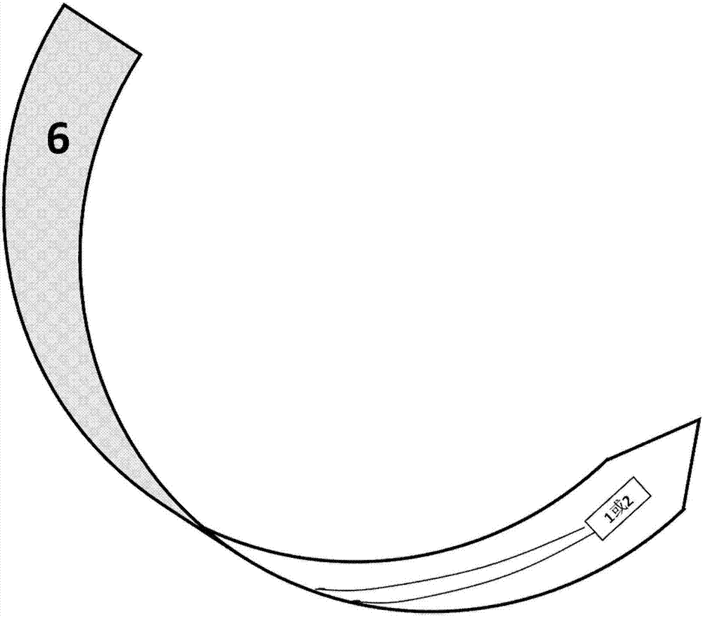
[0043] Such as figure 2 and 3As shown, it is a miniature light stimulation and signal acquisition probe, including a probe substrate 6. The front end of the probe substrate is sharp and sharp, and a light source 1 (photostimulation LED unit) and a sensor 2 (signal signal unit) are integrated at the sharp end at the same time. Acquisition unit), the other end of the probe substrate 6 is a metal contact electrode, through which the probe substrate can be connected to an external circuit, the light source 1 at both ends of the probe substrate 6, the sensor 2 and the electrodes are connected through metal wiring . This kind of probe substrate 6 is a laminated structure, that is, each layer of substrate contains only one control unit (that is, only includes the sensor 2 or only includes the light source 1), such as figure 2 The three layers of substrates shown are stacked, 1 and 2 can be light sources or sensors, and the present invention does not limit the number of layers, an...


PUM


Abstract

The invention discloses a photo-stimulation and signal acquisition probe, which comprises a probe substrate, wherein the probe substrate comprises a front end part and a rear end part, wherein the front end part, which is of a sharp structure, is implanted in an organism, and the front end part is provided with a sensor and a light emitting source; and the rear end part is provided with a sensor electrode electrically connected to a sensor, a light emitting source electrode electrically connected to the light emitting source and a public electrode. The probe provided by the invention, which is simultaneously integrated with a light emitter light emitting unit and a sensor detection unit for photo-stimulation, can facilitate operations.

Description

technical field [0001] The invention relates to a nerve diagnosis and treatment device, in particular to a light stimulation and signal collection probe. Background technique [0002] With the advent of an aging society, senile neurodegenerative diseases such as Alzheimer's and Parkinson's have attracted more and more attention. However, the brain is still the black hole of human cognition. The optogenetics method developed after 2005 can activate or deactivate neural circuits or single neurons in specific brain regions through light. Due to the advantages of real-time, in-situ, fast and reversible light, this method has set off a wave of excitement once it came out. The third revolution in the field of brain science research in the past century, optogenetics technology is known as the most influential technical method of neurobiology in the 21st century. At present, optogenetics is still in the research stage of mice and non-human primates. By implanting LED light probes ...

Claims


Application Information

Patent Timeline
Patent Type & Authority Applications(China)
IPC IPC(8): A61B5/00A61N5/06
CPCA61B5/0059A61B2562/0238A61N5/06
Inventor 詹腾伊晓燕刘志强王军喜李晋闽
Owner INST OF SEMICONDUCTORS - CHINESE ACAD OF SCI
Why Eureka
Try Eureka