Semiconductor structure and formation method thereof

A semiconductor and fin technology, which is applied in the field of semiconductor structure and its formation, can solve the problems of poor resistance performance in the active area of ​​FinFET, and achieve the effect of improving performance

Active Publication Date: 2017-07-07
SEMICON MFG INT (SHANGHAI) CORP +1
View PDF4 Cites 0 Cited by
  • Summary
  • Abstract
  • Description
  • Claims
  • Application Information

AI Technical Summary

Problems solved by technology

[0004] However, existing techniques form FinFETs with poor performance in active area resistance

Method used


Image

  • Semiconductor structure and formation method thereof
  • Semiconductor structure and formation method thereof
  • Semiconductor structure and formation method thereof

Examples


Embodiment Construction

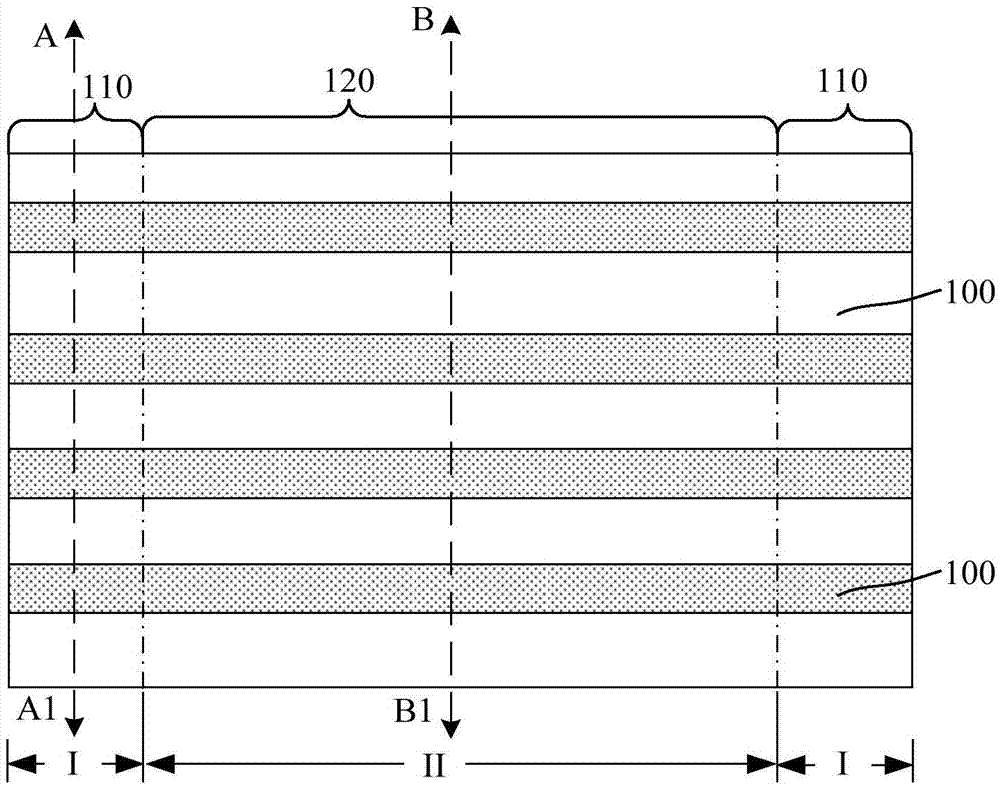
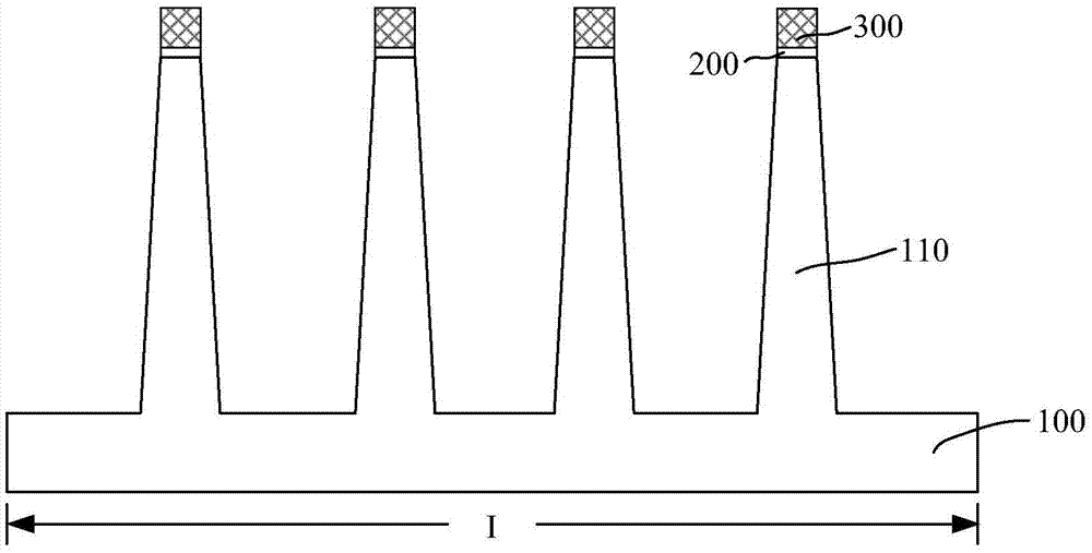
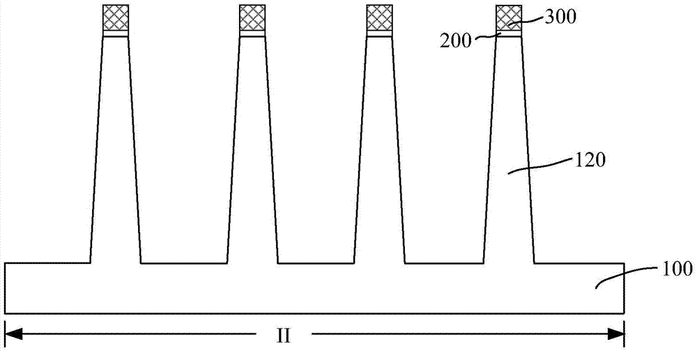
[0030] The resistance performance of the FinFET active region formed in the prior art is poor, and the reason thereof is analyzed in combination with the formation method of the FinFET semiconductor structure in the prior art. The forming method includes the following steps:

[0031] providing a substrate on which fins protruding from the substrate are formed, the fins including a first fin for forming a device and a second fin for forming an active region resistor; After the first fin and the second fin are formed, an isolation layer is formed on the surface of the substrate to cover part of the sidewall surfaces of the first fin and the second fin; A shielding oxide layer is formed on the surface of the second fin, and a threshold voltage adjustment doping process is performed on the first fin; the shielding oxide layer is removed, and a dummy gate oxide layer is formed on the surfaces of the first fin and the second fin and a dummy gate electrode layer to form a dummy gate...


PUM


Abstract

The invention relates to a semiconductor structure and a formation method thereof. The formation method comprises the steps of providing a substrate comprising a first region and a second region and fin portions protruding out of the substrate, wherein a part of the fin portions are located in the first region, the fin portions located in the first region are first fin portions, another part of the fin portions are located in the second region, and the fin portions located in the second region are second fin portions; forming a first isolation layer which covers part of the first fin portions and a second isolation layer which covers the second fin portions at the surface of the substrate between the fin portions, and the top of the first isolation layer is lower than the top of the second isolation layer; doping the second fin portions, and forming an active region resistor inside each second fin portion. According to the invention, the second fin portions are protected through forming the second isolation layer covering the second fin portions at the substrate surface between the second fin portions, and the second fin portions are avoided from being consumed because of being exposed in a process environment of the first fin portions, so that influences imposed on the size of the second fin portions by the process of the first fin portions are avoided, and thus the performance of active region resistors of an FinFET is improved.

Description

technical field [0001] The invention relates to the field of semiconductors, in particular to a semiconductor structure and a forming method thereof. Background technique [0002] In semiconductor manufacturing, with the development trend of VLSI, the feature size of integrated circuits continues to decrease. In order to adapt to the reduction of feature size, the channel length of MOSFET devices is also continuously shortened. However, as the channel length of the device is shortened, the distance between the source and the drain of the device is also shortened, so the control ability of the gate to the channel becomes worse, and the gate voltage pinches off the channel. The difficulty is also increasing, making the phenomenon of subthreshold leakage (subthreshold leakage), the so-called short-channel effect (SCE: short-channel effects) more likely to occur. [0003] Therefore, in order to better adapt to the reduction of feature size, the semiconductor process gradually ...

Claims


Application Information

Patent Timeline
IPC IPC(8): H01L21/336H01L29/78
CPCH01L29/66545H01L29/66795H01L29/78
Inventor 周飞
Owner SEMICON MFG INT (SHANGHAI) CORP
Why Eureka
Try Eureka