Organic light-emitting diode with linearly polarized emission

A technology of light-emitting diodes and organic light-emitting layers, which is applied in the direction of organic light-emitting devices, organic light-emitting device structures, and electric solid-state devices, and can solve the problems of inability to realize the conversion of the polarization mode of OLED devices, complicated preparation process, and high cost of electron beam etching

Active Publication Date: 2017-07-07
HUAIYIN INSTITUTE OF TECHNOLOGY
View PDF10 Cites 8 Cited by
  • Summary
  • Abstract
  • Description
  • Claims
  • Application Information

AI Technical Summary

Problems solved by technology

However, this document reports a metal nanopolarization grating, not a dielectric metal nanopolarization grating structure, and this structure cannot realize the conversion of the internal polarization mod...

Method used


Image

  • Organic light-emitting diode with linearly polarized emission
  • Organic light-emitting diode with linearly polarized emission
  • Organic light-emitting diode with linearly polarized emission

Examples


Embodiment 1

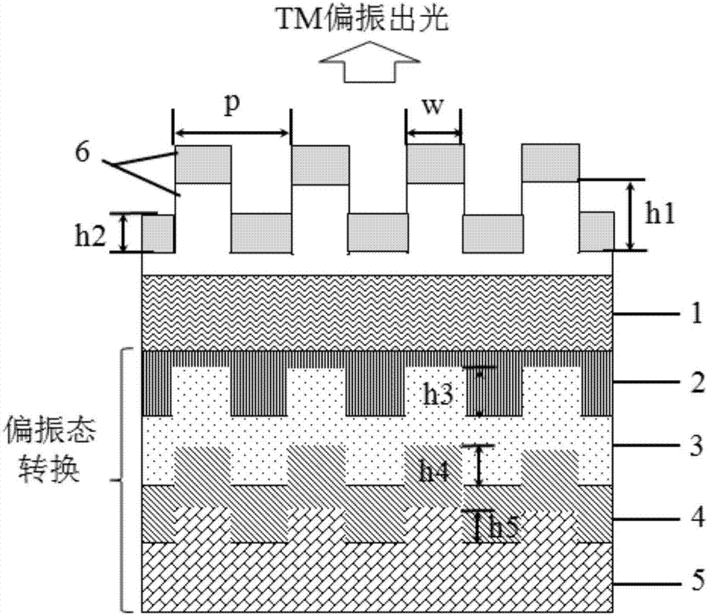
[0031] Taking a flexible and bendable green OLED device (luminescence peak at 520nm) as an example to describe in detail, in this structure, the substrate 1 is the flexible material polyethylene terephthalate / ITO, and the first transport layer 2 is PEDOT :PSS, the organic light-emitting layer 3 is Alq 3: C545T, the second transport layer 4 is Alq3, and the composite back electrode 5 is LiF / Al. The structure of the green OLED device is: polyethylene terephthalate / ITO(120nm) / PEDOT:PSS(80nm) / NPB(40nm) / Alq3:C545T(20nm) / Alq3(40nm) / LiF(1nm) / Al (100nm).

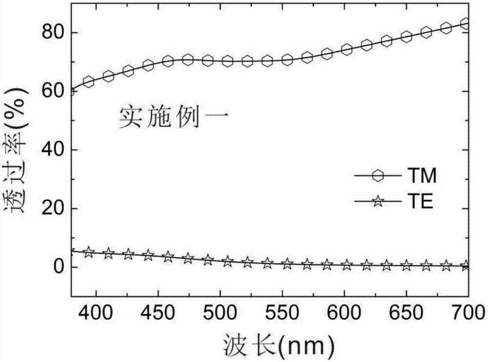
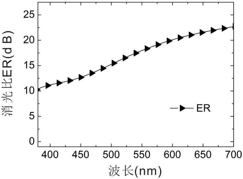
[0032] Firstly, according to the finite element difference algorithm, the morphology of the nano-grating and dielectric metal grating is specifically designed. The optimal polarization extinction ratio and TM wave transmittance of the green light device are judged as criteria. Through theoretical calculation and optimization, the period and duty ratio of the dielectric metal grating of this embodiment are 100nm...

Embodiment 2

[0038] Taking a rigid substrate red OLED device (luminescence peak at 520nm) as an example to describe in detail, in this structure, the substrate 1 is glass / ITO, the first transport layer 2 is a laminated structure of PEDOT:PSS / NPB / TCTA, organic Emitting layer 3 is Ir(MDQ) 2 (acac), the second transport layer 4 is TmPyPB, and the composite back electrode 5 is LiF / Al. The structure of the green OLED device is: glass / ITO(120nm) / PEDOT:PSS(80nm) / NPB(40nm) / TCTA(15nm) / Ir(MDQ) 2 (acac)(0.1nm) / TmPyPB(40nm) / LiF(1nm) / Al(100nm).

[0039] Firstly, according to the finite element difference algorithm, the morphology of the nano-grating and dielectric metal grating is specifically designed. The optimal polarization extinction ratio and TM wave transmittance of the green light device are judged as criteria. Through theoretical calculation and optimization, the period of the nano-grating and the period and duty ratio of the dielectric metal grating in this embodime...


PUM

PropertyMeasurementUnit
Extinction ratioaaaaaaaaaa

Abstract

The invention discloses an organic light-emitting diode (OLED) with linearly polarized emission, and belongs to the technical field of organic photoelectric display devices. The OLED comprises a substrate, a first transport layer, an organic light-emitting layer, a second transport layer and a composite back electrode which are sequentially arranged from the top down, wherein nano grating structures are respectively arranged on the first transport layer, the organic light-emitting layer, the second transport layer and the composite back electrode; the nano grating structures are periodic array gratings; a period of each grating is 70-180nm; a duty ratio of each grating is 0.4-0.7; the groove depth of each grating is 20-80nm; and a metal dielectric nano polarized grating structure is arranged on the upper surface of the substrate. The OLED with the linearly polarized emission realizes direct linearly polarized emission of an OLED device; a preparation technology of the OLED device is compatible with low-cost soft nanoimprint photolithography; and the OLED device is applicable to rigid, flexible and tensile substrate materials, and has a potential practical value in the fields of linearly polarized light navigation, target counter-stealth, identification and the like.

Description

technical field [0001] The invention belongs to the technical field of organic photoelectric display devices, and in particular relates to a linearly polarized light emitting organic light emitting diode. Background technique [0002] In recent years, the display technology of light emitting diode (LED) has gradually replaced the mainstream position of traditional liquid crystal display (LCD) and cathode ray tube (CRT) (display technology. However, with the rise of organic light emitting diode (OLED) technology, The status of LED is also under potential threat, mainly because OLED technology has many incomparable advantages of traditional LED, which can stand out. Specifically, OLED has self-illumination, wide viewing angle (up to 175° or more), and fast response speed (1μs) , high luminous efficiency, wide color gamut and low working voltage (about 3-10V), its panel (thickness can be less than 1mm) can be made into large-size flexible or stretchable panels, and the producti...

Claims


Application Information

Patent Timeline
IPC IPC(8): H01L51/52H01L51/50
CPCH10K50/00H10K50/80H10K50/85H10K50/868H10K2102/301H10K2102/302
Inventor 周雷高本领范媛媛宋光张俊
Owner HUAIYIN INSTITUTE OF TECHNOLOGY
Why Eureka
Try Eureka