

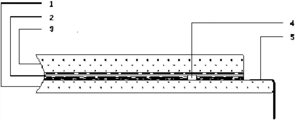
LED glass laminating structure and glass processing laminating technology thereof
A technology of LED glass and sheet structure, which is applied in the field of photoelectric glass and video, which can solve the problems of easily broken lines or flexible circuit boards, the inability to perform secondary repairs, and poor connection of lead wires, etc. Novelty, easy to clean effect
- Summary
- Abstract
- Description
- Claims
- Application Information
AI Technical Summary
Problems solved by technology
Method used
Image

Examples
Embodiment
[0036] The specific method of glass production lamination process is as follows:
[0037] a. Before etching, conduct a visual inspection of the state of the conductive film on the underlying conductive glass;
[0038] b. The bottom conductive glass adopts the scanning method of the sub-region to carry out the laser etching circuit;
[0039] c. Visually inspect the conductive film circuit of the bottom conductive glass after etching, and analyze whether the conductive film circuit is short-circuited or open-circuited according to the collected data, and whether there is damage or damage;
[0040] d. After etching the circuit, use a large LED photoelectric glass placement machine for LED placement;
[0041] e. After the LED mounting is completed, the bottom conductive glass directly enters the UV curing equipment for curing;
[0042] f. The bottom conductive glass after UV curing is completed and then enters the silver paste curing equipment for curing;
[0043] g. Conduct po...
PUM
 Abstract
Description
Claims
Application Information