Method for improving performance of fin field-effect transistor

A fin field effect transistor and performance technology, which is applied in electrical components, semiconductor/solid-state device manufacturing, circuits, etc., can solve the problem that the electrical performance of fin field effect transistors needs to be improved, achieve weak diffusion barrier ability, and improve doping. Efficient and protective effect

Inactive Publication Date: 2017-07-14
SEMICON MFG INT (SHANGHAI) CORP +1
View PDF7 Cites 10 Cited by
  • Summary
  • Abstract
  • Description
  • Claims
  • Application Information

AI Technical Summary

Problems solved by technology

[0005] However, the electrical performance of the fin field effect transistor formed by the prior art needs to be improved

Method used


Image

  • Method for improving performance of fin field-effect transistor
  • Method for improving performance of fin field-effect transistor
  • Method for improving performance of fin field-effect transistor

Examples


Embodiment Construction

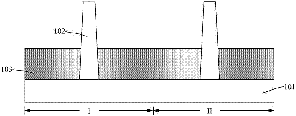
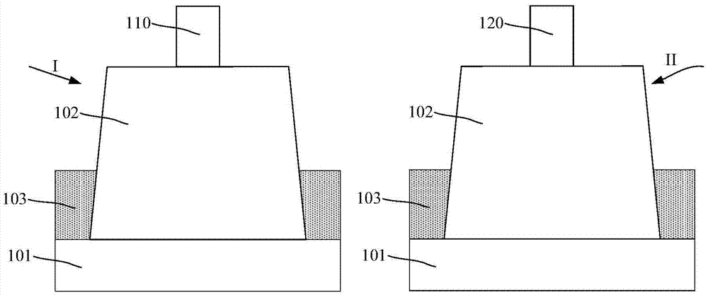
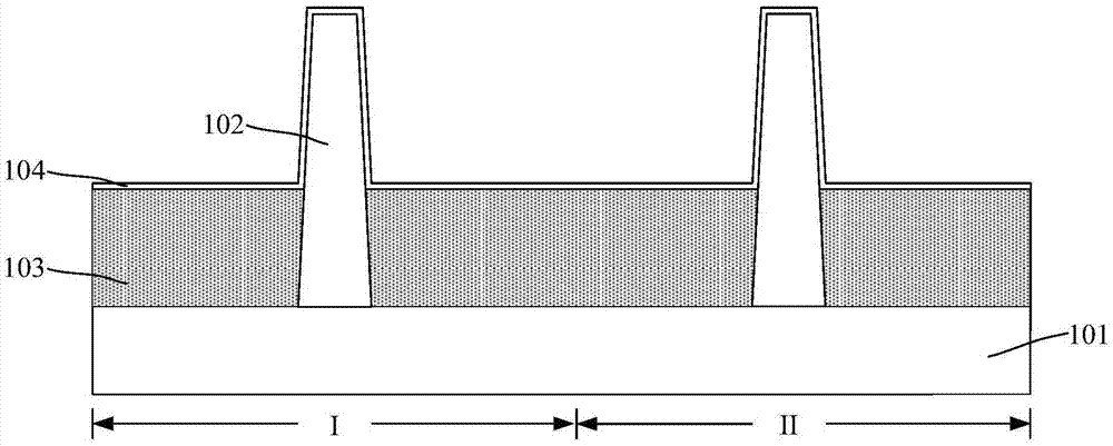
[0023] Studies have found that in order to improve the electrical performance of FinFETs, it is usually necessary to do doping on the fins of FinFETs, for example, doping the fins to form lightly doped regions (LDDs), or , doping the fins to form heavily doped regions, the heavily doped regions being the source and drain regions, or performing doping on the fins to form a threshold voltage adjustment region to adjust the fin field effect transistor formed threshold voltage. Generally, the doping treatment is performed by using an ion implantation process (Implant). However, the ion implantation process is likely to cause implantation damage to the surface of the fin, resulting in poor morphology and lattice damage of the fin, and also easily leads to Ions are implanted in undesired areas of the interior. For this reason, a method of solid source doping (SSD, Solid Source Doping) is proposed, specifically, a doped layer is formed on the surface of the fin, and there are doping...


PUM


Abstract

A method for improving performance of a fin field-effect transistor comprises the steps of providing a substrate, wherein discrete fin parts are formed on a surface of the substrate, an isolation layer is also formed on the surface of the substrate and covers surfaces of a part of side walls of the fin parts, and the top of the isolation layer is lower than the tops of the fin parts; forming a gate structure bridging the fin parts on a surface of the isolation layer, wherein the gate structure covers the surfaces of a part of tops and the side walls of the fin parts; forming an amorphous material layer covering the surfaces of a part of tops and the side walls of the fin parts and the surface of the isolation layer; forming an oxide doping layer on a surface of the amorphous material layer; annealing the oxide doping layer so that doping ions are diffused and enter the fin parts, and forming doping regions in the fin parts at two sides of the gate structure; and removing the oxide doping layer. During the process of removing the oxide doping layer, the amorphous material layer has a protection effect on the isolation layer, the etching loss caused by the technology of removing the oxide doping layer on the isolation layer is prevented, so that the thickness of the isolation layer is maintained unchanged, and the electrical property of the formed fin field-effect transistor is further improved.

Description

technical field [0001] The invention relates to the technical field of semiconductor manufacturing, in particular to a method for improving the performance of a fin field effect transistor. Background technique [0002] With the continuous development of semiconductor process technology, the development trend of semiconductor process nodes following Moore's Law continues to decrease. In order to adapt to the reduction of process nodes, the channel length of MOSFET field effect transistors has to be continuously shortened. The shortening of the channel length has the advantages of increasing the die density of the chip and increasing the switching speed of the MOSFET field effect tube. [0003] However, as the channel length of the device is shortened, the distance between the source and the drain of the device is also shortened, so that the control ability of the gate to the channel becomes worse, resulting in the phenomenon of subthreshold leakage, namely So-called short-...

Claims


Application Information

Patent Timeline
Patent Type & Authority Applications(China)
IPC IPC(8): H01L21/225H01L21/8238H01L21/336
CPCH01L29/66803H01L21/225H01L21/823821
Inventor 李勇
Owner SEMICON MFG INT (SHANGHAI) CORP
Why Eureka
Try Eureka