Low-voltage differential signaling receiving interface and low-voltage differential signaling receiving method
A low-voltage differential and signal receiving technology, applied in electrical digital data processing, instruments, etc., can solve the problems of indeterminate sampling delay time and inability to receive data correctly
- Summary
- Abstract
- Description
- Claims
- Application Information
AI Technical Summary
Problems solved by technology
Method used
Image
Examples
Embodiment 1
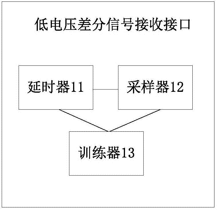
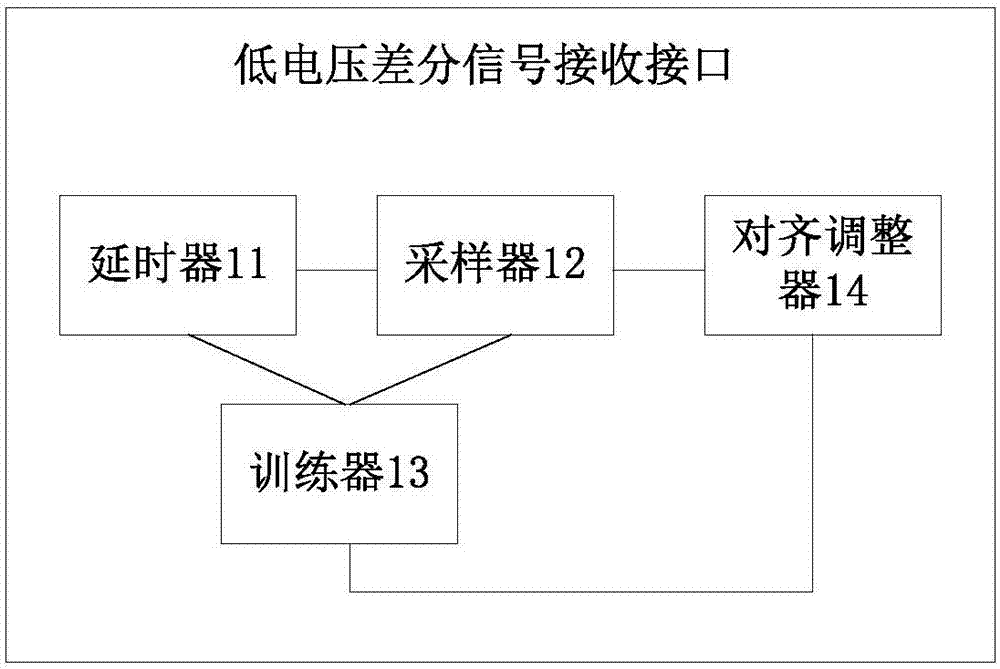
[0024] This embodiment provides a low-voltage differential signal receiving interface, the low-voltage differential signal receiving interface can be realized by using FPGA (Field-Programmable Gate Array, Field Programmable Gate Array) resources, and the low-voltage differential signal receiving interface can Low-voltage differential signal reception for multiple rates. Of course, the low-voltage differential signal receiving interface in this embodiment is not limited to be realized by FPGA, and may also be realized by other methods. For the low voltage differential signal receiving interface in this embodiment, see figure 1 shown, which includes:
[0025] The delayer 11 is used for delaying the serial sample data (pattern) sent by the sender according to the preset delay step step.
[0026] Delay device 11 in the present embodiment can be realized by the input / output delay unit (IO DELAY) of FPGA, also can realize by other time-delay function circuits certainly; (That is,...
Embodiment 2
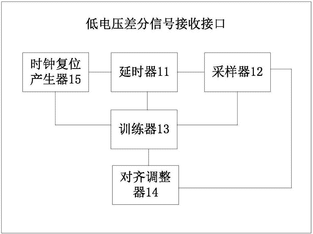
[0046] In order to better understand the present invention, this embodiment provides a more specific low-voltage differential signal receiving interface, please refer to image 3 As shown, it includes a delayer 11 , a sampler 12 , a trainer 13 , an alignment adjuster 14 and a clock reset generator 15 . See Figure 4 As shown, the reset generator 15 in this embodiment may include a clock controller 151 , a clock switch enable controller 152 , a clock switch 153 , and a clock division controller 154 . It should be understood that one sampler 12 in this embodiment corresponds to one delayer 11, and there may be multiple sets of delayers 11 and samplers 12 in one low-voltage differential signal receiving interface.
[0047] The delay device 11 in this embodiment is realized by a dedicated input / output delay unit inside the FPGA, and is used to delay the serial sample data sent by the sender according to the preset delay step step. In this embodiment The delay adjustment range of...
Embodiment 3
[0063] This embodiment provides a low voltage differential signal receiving method, please refer to Figure 7 shown, including:
[0064] S701: Perform delay processing on the serial sample data sent by the sender according to a preset delay step.
[0065] The S601 step in the present embodiment can be realized by the input / output delay unit (IO DELAY) of FPGA, certainly also can realize by other delay function circuits; The number of delay steps N) can be flexibly set, for example, it can be set to 128 steps or 256 steps according to actual needs. When the serial sample data sent by the sender is delayed according to the preset delay step, it is gradually adjusted until the corresponding data boundary is found or until the maximum number of delay steps N is reached, and each delay step in this embodiment The specific value of the long step can also be flexibly set according to specific needs, for example, it can be set to 25ps, or 50ps, and so on.
[0066] S702: Sampling th...
PUM
 Abstract
Description
Claims
Application Information
 - R&D
- Intellectual Property
- Life Sciences
- Materials
- Tech Scout
- Unparalleled Data Quality
- Higher Quality Content
- 60% Fewer Hallucinations
Browse by: Latest US Patents, China's latest patents, Technical Efficacy Thesaurus, Application Domain, Technology Topic, Popular Technical Reports.
© 2025 PatSnap. All rights reserved.Legal|Privacy policy|Modern Slavery Act Transparency Statement|Sitemap|About US| Contact US: help@patsnap.com


