
PCB manufacturing method for conveniently detecting back drilling hole precision

A manufacturing method and back-drilling technology, applied in printed circuit manufacturing, circuit inspection/identification, and electrical connection formation of printed components, etc., can solve the problem of X-ray failure to illuminate the offset, back-drilling offset, drilling and disconnecting lines and other problems, to achieve the effect of saving detection costs and labor costs, improving work efficiency, and convenient and simple accuracy

Active Publication Date: 2017-07-18
SHENZHEN SUNTAK MULTILAYER PCB
View PDF3 Cites 7 Cited by
  • Summary
  • Abstract
  • Description
  • Claims
  • Application Information

AI Technical Summary

Problems solved by technology

In the actual production and processing process, offsets often occur when back drilling is processed. When the alignment between back drilling and primary drilling is poor, the length of the short line will be larger and smaller at the slightest level, and the drilled line will be broken if it is severe. or broken holes
Not only can't achieve the expected effect, affect the accuracy of back drilling, but also produce defective products, which will increase the cost. This shows the importance of back drilling alignment
[0004] At present, the alignment of back-drilled holes is confirmed mainly through X-ray inspection after back-drilling. This method has the following defects: 1. The offset value of back-drilled holes cannot be accurately known; 2. If each layer has Copper, if the total copper thickness is thicker, the X-ray will not be able to see the offset

Method used


Image

  • PCB manufacturing method for conveniently detecting back drilling hole precision
  • PCB manufacturing method for conveniently detecting back drilling hole precision
  • PCB manufacturing method for conveniently detecting back drilling hole precision

Examples


Embodiment

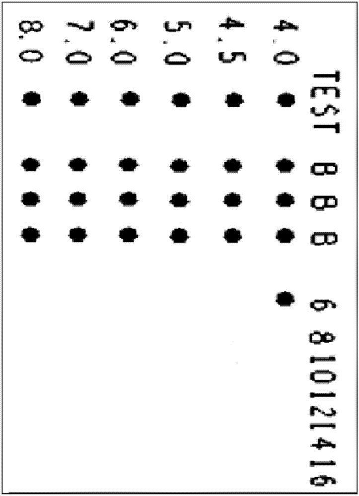
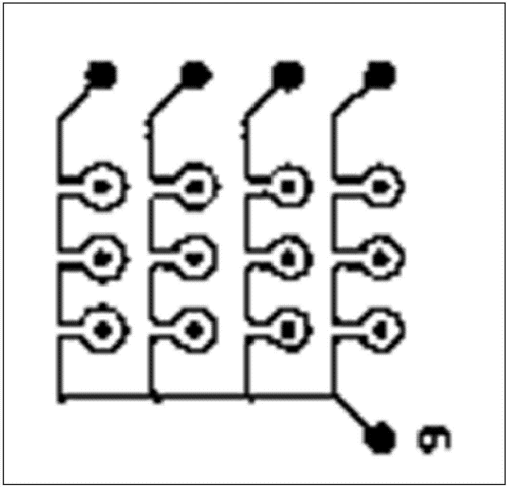
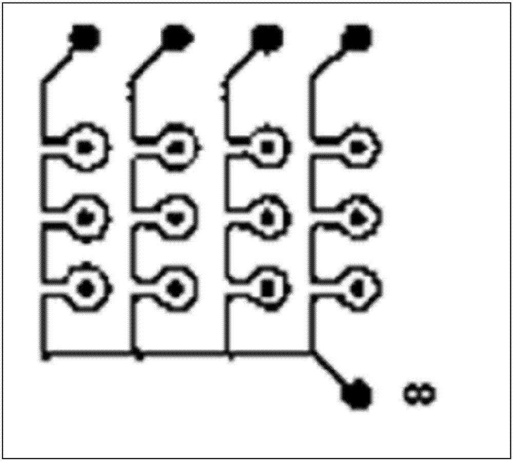
[0026] refer to Figure 1 to Figure 3 , the present invention provides a kind of method for making the PCB that is convenient to detect back drilling accuracy, and concrete steps are as follows:

[0027] According to the existing technology, the substrate is made into a production board with an outer circuit by successively cutting the material → negative film process to make the inner layer circuit → pressing → drilling → sinking copper → full board electroplating → positive film process to make the outer layer circuit. details as follows:

[0028] a. Cutting: Cut out the core board according to the panel size 520mm×620mm, and the thickness of the core board is 0.5mm H / H.

[0029] b. Inner layer circuit (negative film process): produced by vertical coating machine, the film thickness is controlled to 8μm, and a fully automatic exposure machine is used to complete the exposure of the inner layer circuit with 5-6 grid exposure rulers (21 grid exposure rulers), and then etch af...


PUM


Abstract

The invention relates to the field of printed circuit board manufacturing and specifically relates to a PCB manufacturing method for conveniently detecting back drilling hole precision. According to the method, an open loop conductive annular line is arranged around each back drilling position; after back drilling operation is completed, a universal meter is used for detecting whether the annular line is open or not via detection points; if the annular line is open, the annular line is broken via drilling operation; if the annular line is short circuited, the annular line is not broken via the drilling operation. Via measurement, identification marks of short circuits are written down, and the identification marks indicate numerical values of distance between back drilling holes and annular lines and numbers of layers on which the annular lines are positioned; via common add-and-subtract operation, accurate offset can be known in a visual manner, and back drilling hole precision can be read in a simple and convenient manner. When the back drilling holes are large in quantity, poor quality holes can be identified easily. Via use of the method, simple operation can be achieved, detection cost and man power cost can be greatly lowered, and working efficiency can be improved.

Description

technical field [0001] The invention relates to the field of printed circuit board manufacturing, in particular to a PCB manufacturing method which is convenient for detecting the accuracy of back drilling. Background technique [0002] PCB (Printed Circuit Board), the Chinese name is printed circuit board, also known as printed circuit board. The PCB is a support for electronic components and provides electrical connections for electronic components. The production process of PCB is generally: material cutting → inner layer pattern transfer → inner layer etching → lamination → drilling → sinking copper → whole board plating → outer layer pattern transfer → pattern plating → etchingsolder mask → surface treatment → forming processing etc. [0003] In the PCB manufacturing process, especially in the high-speed PCB processing process, in order to prevent signal distortion or delay, it is necessary to drill off the hole wall metal that does not play any connection or trans...

Claims


Application Information

Patent Timeline
Patent Type & Authority Applications(China)
IPC IPC(8): H05K3/00H05K3/42H05K1/02
CPCH05K1/0268H05K3/0047H05K3/429H05K2203/0214
Inventor 翟青霞彭卫红刘东
Owner SHENZHEN SUNTAK MULTILAYER PCB
Learn More