Supercharge Your Innovation With Domain-Expert AI Agents!

Overdrive amplifier and semiconductor device

An overdrive and amplifier technology, applied to amplifiers, amplifiers with semiconductor devices/discharge tubes, instruments, etc., can solve problems such as difficulty in high speed, delayed convergence time, and poor convergence time

Active Publication Date: 2021-01-05
SYNAPTICS JAPAN GK
View PDF13 Cites 0 Cited by
  • Summary
  • Abstract
  • Description
  • Claims
  • Application Information

AI Technical Summary

Problems solved by technology

The resistance component and the capacitance component of the liquid crystal display element are distributed in the source line, and the load component of the remote end becomes larger. Even if the drive amplifier is operated at high speed, the convergence time at the near end of the load is short. There is also a difference in the convergence time of the remote end of the load, and the convergence time of the remote end tends to be delayed
When the panel load is large, the RC of the panel load dominates the convergence time at the far end of the load, and even if the drive amplifier is increased in speed, it is difficult to increase the speed of the drive amplifier.
[0003] The difference in the drive convergence time between the near end and the far end of the load is noticeable depending on the size of the liquid crystal display panel, the size of the allowable power consumption, etc., and the difference may also occur in a low temperature environment

Method used


Image

  • Overdrive amplifier and semiconductor device
  • Overdrive amplifier and semiconductor device
  • Overdrive amplifier and semiconductor device

Examples


Embodiment Construction

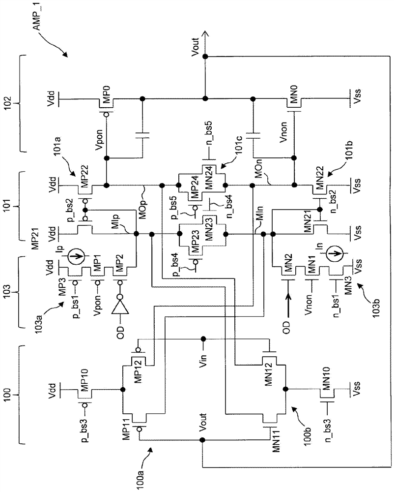
[0093] In the following, various overdrive amplifiers exemplified by AMP_1 to AMP_8 will be described. Each of the overdrive amplifiers AMP_1 to AMP_8 includes a differential input circuit 100, a current mirror load 101, an output circuit 102, and an overdrive circuit 103, and constitutes a buffer amplifier such as a voltage follower amplifier. The overdrive circuit 103 is realized by a bias current circuit through which a bias current flows during overdrive.

[0094] "Overdrive Amplifier AMP_1"

[0095] based on figure 1 The overdrive amplifier AMP_1 of the first example will be described.

[0096] In this overdrive amplifier ASMP_1, although the current mirror load 100 is not particularly limited, a pMOS current mirror circuit 101a connected between a floating current source 101c and a high-potential power supply Vdd (for example, a positive power supply such as +15V) , and an nMOS current mirror circuit 101b connected between the floating current source 101c and the low-po...


PUM


Abstract

The present invention relates to an overdrive amplifier and a semiconductor device. An overdrive amplifier that satisfies both low current consumption and high-speed drive can be realized by adding a small-scale circuit. The overdrive amplifier has: a differential input circuit (100) having an input transistor (MP12, MN12) supplying an input signal to a gate and a feedback input transistor (MP11, MN11) feeding back an output signal to the gate as a pair of differential input transistors a current mirror load (101) with a mirrored input current path connected to the current path of the feedback input transistor and a mirrored output current path connected to the current path of the input transistor; input and output from the mirrored output current path of the current mirror load an output circuit (102) of a control signal; and a bias current (Ip, In) that enhances a direction of an output of the output circuit using the output control signal during overdrive to flow through the An overdrive circuit (103) for a current mirror load.

Description

technical field [0001] The present invention relates to an overdrive amplifier, and further relates to a semiconductor device including the overdrive amplifier, and relates to effective technology applied to an LCD (liquid crystal display) driver IC (Integrated Circuit, for example). Background technique [0002] The drive performance of a load driven by a buffer amplifier or the like differs between the near end and the far end of the load, and also differs depending on the temperature of the load. For example, in a liquid crystal display panel, a plurality of liquid crystal display elements are arranged in a matrix in the row and column directions, the gate lines are connected to the selection terminals of the liquid crystal display elements in units of display rows in the row direction, and the source lines are connected in units of column directions. It is used as the data terminal of the liquid crystal display element. A plurality of source lines are driven by a drivin...

Claims


Application Information

Patent Timeline
Patent Type & Authority Patents(China)
IPC IPC(8): G09G3/36
CPCG09G3/36G09G3/3688G09G2310/0291H03F3/45219H03F3/45636H03F2203/45116H03F2203/45154H03F2203/45674G09G3/3648G09G3/3696G09G2300/0819G09G2330/021
Inventor 佐伯穣
Owner SYNAPTICS JAPAN GK
Features
  • R&D
  • Intellectual Property
  • Life Sciences
  • Materials
  • Tech Scout
  • Unparalleled Data Quality
  • Higher Quality Content
  • 60% Fewer Hallucinations
Learn More