

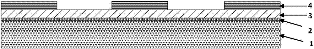
Manufacturing method for patterned sensitive metal or metal oxide material
A technology of sensitive metals and processing methods, which is applied in the manufacture of electrical components, circuits, semiconductors/solid-state devices, etc., and can solve problems such as device performance impact
- Summary
- Abstract
- Description
- Claims
- Application Information
AI Technical Summary
Problems solved by technology
Method used
Image

Examples
Embodiment 1
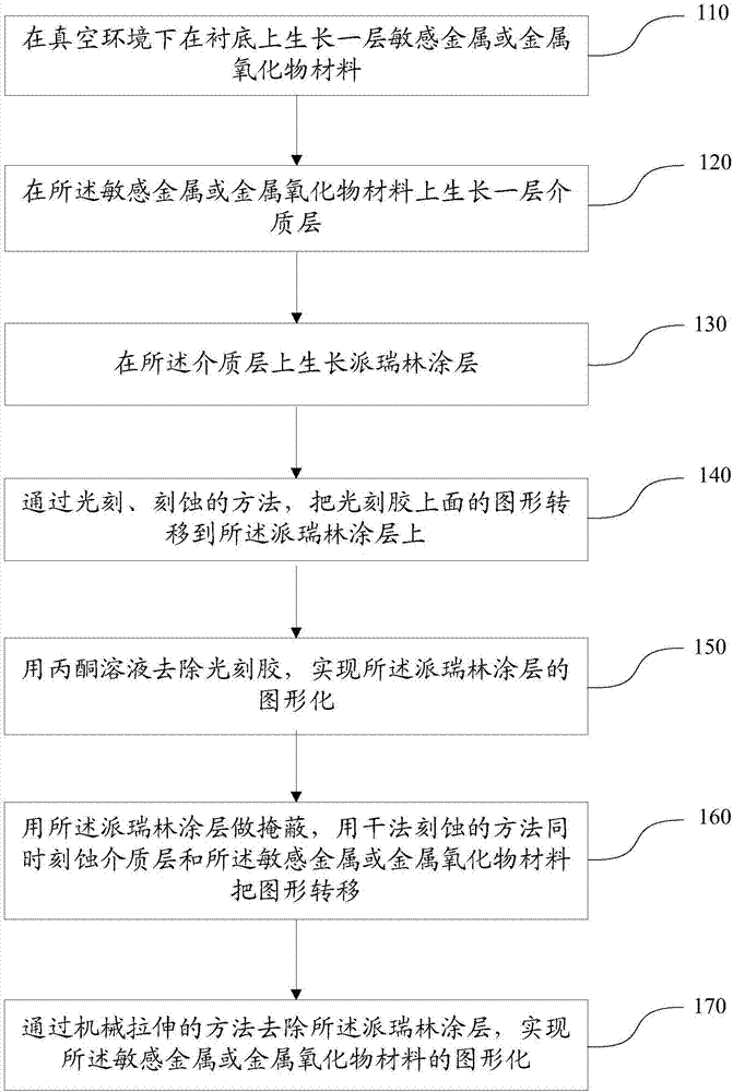
[0047] Embodiment 1: A processing method based on patterning of the sensitive metal Mg electrode cossbar structure, the specific steps are as follows:
[0048] Step 201: Sputtering a layer of Mg metal in a vacuum environment and covering it with a layer of Al 2 o 3 Dielectric layer, and then grow a layer of lower electrode through conventional photolithography, evaporation, and stripping processes, and then grow a parylene coating, and then photolithography, etching, and stripping processes to transfer the pattern on the photoresist to parylene on the coating;
[0049] Step 202: Use the parylene coating as a mask, and use Ar plasma physical etching method to etch away the Al 2 o 3 The dielectric layer and the Mg metal layer are patterned, and then the parylene coating is removed by mechanical stretching to realize the patterning of the cossbar structure of the Mg electrode.
Embodiment 2
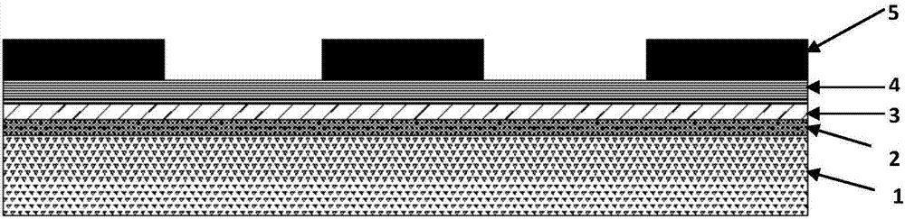
[0050] Embodiment 2: A processing method based on metal oxide MgO patterning, the specific steps are as follows.
[0051] Step 301: sputtering a layer of MgO in a vacuum environment to cover a layer of SiO 2 Dielectric layer, and then grow the parylene coating, and then transfer the pattern on the photoresist to the parylene coating through photolithography, etching, and stripping processes;
[0052]Step 302: Use the parylene coating as a mask, and use Ar plasma physical etching to etch away the SiO 2 The dielectric layer and MgO are patterned, and then the parylene coating is removed by mechanical stretching.
[0053] One or more technical solutions provided in the embodiments of the present invention have at least the following technical effects or advantages:
[0054] The embodiment of the present invention is processed in a vacuum environment, and the contact between the sensitive metal and metal oxide materials and the air is avoided as much as possible; in the process ...
PUM
 Abstract
Description
Claims
Application Information