Fan-out-type wafer-level packaging structure and preparation method therefor

A wafer-level packaging, fan-out technology, used in semiconductor/solid-state device manufacturing, semiconductor/solid-state device components, semiconductor devices, etc., which can solve the problems of long flip-chip communication response time, packaging failure, offset and other problems , to achieve the effect of shortening communication response time, ensuring device performance, and increasing yield

Inactive Publication Date: 2017-07-25
SJ SEMICON JIANGYIN CORP
View PDF4 Cites 6 Cited by
  • Summary
  • Abstract
  • Description
  • Claims
  • Application Information

AI Technical Summary

Problems solved by technology

[0005] In view of the above-mentioned shortcomings of the prior art, the object of the present invention is to provide a fan-out wafer level packaging structure and a preparation method thereof, which are used to solve the problem of flip-chip in the fan-out wafer level packaging structure in the prior art. The problem of long communication response time between flip-chips caused by the single-layer arrangement of chips, and the problem of over-implantation caused by the formation of solder bumps directly on the surface of the plastic packaging material layer or the surface of the rewiring layer through the lower metallization layer. During the ball reflow process, the solder ball bumps in the ball drop state are easy to move and shift in position, which affects the device performance of the fan-out wafer level packaging structure, and even leads to packaging failure.

Method used


Image

  • Fan-out-type wafer-level packaging structure and preparation method therefor
  • Fan-out-type wafer-level packaging structure and preparation method therefor
  • Fan-out-type wafer-level packaging structure and preparation method therefor

Examples


Embodiment 1

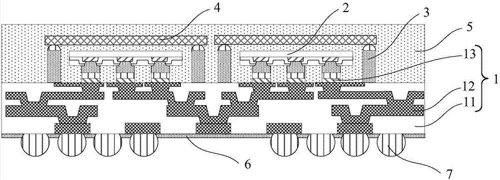
[0086] see figure 1 , the present invention provides a fan-out wafer level packaging structure, the fan-out wafer level packaging structure at least includes: a rewiring layer 1; a first flip chip 2, the first flip chip 2 bonding on the upper surface of the rewiring layer 1 and is electrically connected to the rewiring layer 1; a metal connecting column 3, the metal connecting column 3 is bonded to the upper surface of the rewiring layer 1, and is connected to the The rewiring layer 1 is electrically connected; the second flip chip 4, the second flip chip 4 is bonded to the upper surface of the metal connecting column 3, and is located above the first flip chip 2, the The second flip chip 4 is electrically connected to the rewiring layer 1 via the metal connecting column 3; the plastic sealing layer 5 is located on the upper surface of the rewiring layer 1 and fills the first Flip chip 2, the metal connecting column 3, the gap between the second flip chip 4 and the rewiring l...

Embodiment 2

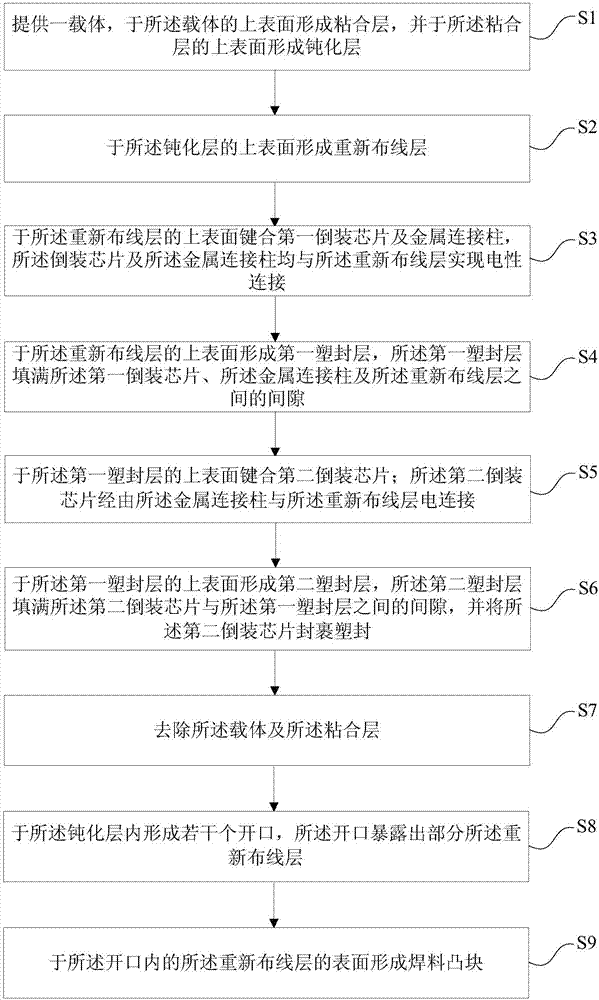
[0106] see image 3 , the present invention also provides a method for preparing a fan-out wafer-level packaging structure, the method for preparing a fan-out wafer-level packaging structure is suitable for preparing the fan-out wafer-level packaging as described in Embodiment 1 structure, the preparation method of the fan-out wafer level packaging structure at least includes the following steps:

[0107] S1: providing a carrier, forming an adhesive layer on the upper surface of the carrier, and forming a passivation layer on the upper surface of the adhesive layer;

[0108] S2: forming a rewiring layer on the upper surface of the passivation layer;

[0109] S3: bonding a first flip chip and a metal connecting post on the upper surface of the rewiring layer, and both the flip chip and the metal connecting post are electrically connected to the rewiring layer;

[0110] S4: forming a first plastic encapsulation layer on the upper surface of the rewiring layer, the first plasti...


PUM


Abstract

The invention provides a fan-out-type wafer-level packaging structure and a preparation method therefor. The structure comprises a rewiring layer; a first flip chip which is bonded to the upper surface of the rewiring layer; a metal connecting column which is bonded to the upper surface of the rewiring layer; a second flip chip which is bonded to the upper surface of the metal connecting column; a plastic packaging layer which is located on the upper surface of the rewiring layer; a passivation layer which is located on the lower surface of the rewiring layer, wherein the interior of the passivation layer is provided with a plurality of openings; a welding ball convex block which is located in the opening, and is electrically connected with the rewiring layer. In the structure, the lower surface of the rewiring layer is provided with the passivation layer, and the passivation layer can effectively prevent the welding ball convex block in a ball dripping state from moving in a reballing backflow process, thereby guaranteeing the performance of a device in the structure, and improving the yield.

Description

technical field [0001] The invention relates to the technical field of semiconductor packaging, in particular to a fan-out wafer-level packaging structure and a preparation method thereof. Background technique [0002] Lower cost, more reliable, faster and higher density circuits are the goals pursued by integrated circuit packaging. In the future, integrated circuit packaging will increase the integration density of various electronic components by continuously reducing the minimum feature size. Currently, advanced packaging methods include: Wafer Level Chip Scale Packaging (WLCSP), Fan-Out Wafer Level Package (FOWLP), Flip Chip, Package on Package (Package on Package, POP) and so on. [0003] Fan-out wafer-level packaging is an embedded chip packaging method for wafer-level processing. It is currently one of the advanced packaging methods with more input / output ports (I / O) and better integration flexibility. Compared with conventional wafer-level packaging, fan-out wafe...

Claims


Application Information

Patent Timeline
Patent Type & Authority Applications(China)
IPC IPC(8): H01L23/488H01L21/60H01L25/18
CPCH01L24/16H01L24/81H01L25/18H01L2224/0231H01L2224/02331H01L2224/02381H01L2224/02379H01L2224/16145H01L2224/81007H01L2224/81005H01L2224/97H01L2924/15192H01L2924/15311H01L2924/18161H01L21/568H01L2224/16225H01L2224/16235
Inventor 吴政达林正忠
Owner SJ SEMICON JIANGYIN CORP
Why Eureka
Try Eureka