Manufacturing method for color micro-light-emitting diode array substrate

A technology for micro-light-emitting diodes and array substrates, which is applied to electrical components, electrical solid-state devices, circuits, etc., can solve the problems of limiting the number of MicroLEDs, inability to realize multi-color MicroLED arrangement, and difficult to colorize LED display arrays, and achieves a manufacturing method. Simple and easy effects

Inactive Publication Date: 2017-08-04
SHENZHEN CHINA STAR OPTOELECTRONICS TECH CO LTD
View PDF10 Cites 57 Cited by
  • Summary
  • Abstract
  • Description
  • Claims
  • Application Information

AI Technical Summary

Problems solved by technology

[0005] Aiming at the problems existing in the micro-transfer printing using the transfer head, a chip bonding (Chip Bonding) technology has been proposed in the field to transfer the Micro LED array, that is, the supply substrate of the Micro LED is directly aligned with the receiving substrate And bonding, saving the intermediate steps of the transfer head, but it is difficult to realize the colorization of the LED display array, because most of the Micro LEDs grown on...

Method used


Image

  • Manufacturing method for color micro-light-emitting diode array substrate
  • Manufacturing method for color micro-light-emitting diode array substrate
  • Manufacturing method for color micro-light-emitting diode array substrate

Examples


Embodiment Construction

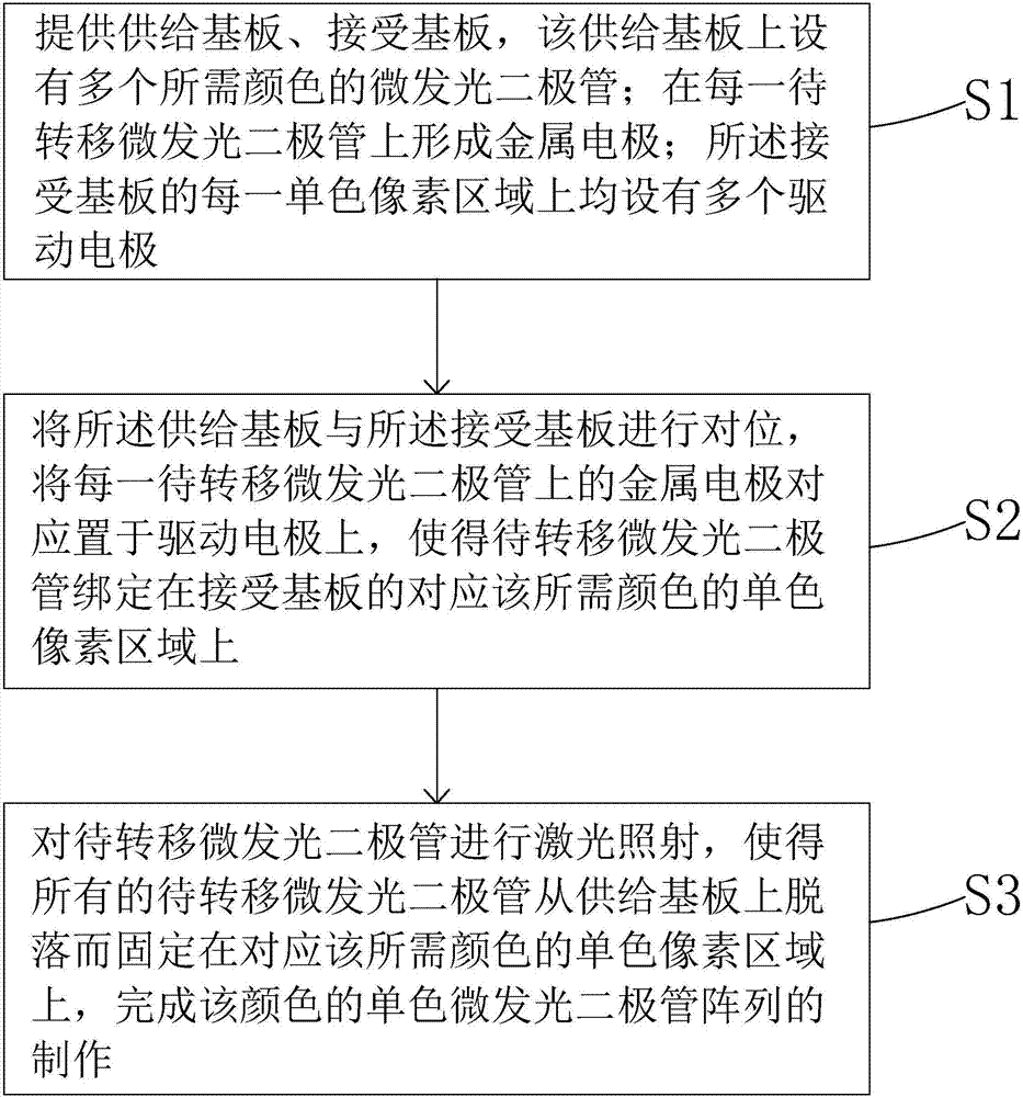
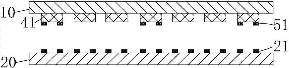
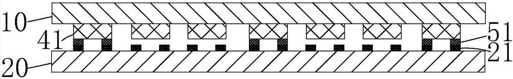
[0035] In order to further illustrate the technical means adopted by the present invention and its effects, the following describes in detail in conjunction with preferred embodiments of the present invention and accompanying drawings.

[0036] The present invention provides a method for manufacturing a color micro-light emitting diode array substrate. The color micro-light emitting diode array substrate includes a receiving substrate 20 and a color micro-light emitting diode array arranged on the receiving substrate 20; the receiving substrate 20 includes A plurality of monochrome pixel areas respectively corresponding to different colors, the color micro-light emitting diode array includes a plurality of monochrome micro-light-emitting diode arrays of different colors, and the monochrome micro-light-emitting diode array of each color is set on the pixel area.

[0037] see figure 1 , wherein, the manufacturing method of the single-color micro-light-emitting diode array of ea...


PUM


Abstract

The invention provides a manufacturing method for a color micro-light-emitting diode array substrate, and the method comprises the steps: manufacturing a plurality of color micro-light-emitting diode arrays which are respectively formed by a plurality of single-color micro-light-emitting diode arrays with different colors on a receiving substrate, wherein the manufacturing of the single-color micro-light-emitting diode array with one color is combined with the binding technology and the laser falling-off technology; selectively forming a metal electrode on the micro-light-emitting diode in a specific region on a feeding substrate, selectively binding the micro-light-emitting diode in the specific region on the receiving substrate, and selectively carrying out laser irradiation of the micro-light-emitting diode in the specific region, thereby enabling the micro-light-emitting diode in the specific region to be separated from the feeding substrate through binding and laser annealing; forming the single-color micro-light-emitting diode arrays on the receiving substrate, thereby achieving the manufacturing of the single-color micro-light-emitting diode arrays with different colors on the receiving substrate. Moreover, the manufacturing method is simple and easy.

Description

technical field [0001] The invention relates to the field of display technology, in particular to a method for manufacturing a color micro-light emitting diode array substrate. Background technique [0002] Micro LED (Micro LED) is a device with a size between several microns and hundreds of microns. Because it is much smaller than ordinary LEDs, it is possible to use a single LED as a pixel (Pixel) for display. A Micro LED display is a display that uses a high-density Micro LED array as a display pixel array to achieve image display. Like a large-scale outdoor LED display, each pixel can be addressed and individually driven to light up. It can be regarded as a A reduced version of the outdoor LED display, which reduces the pixel distance from millimeters to microns. Micro LED displays are self-luminous displays like Organic Light-Emitting Diode (OLED) displays, but Micro LED displays are compared to OLED displays also have the advantages of better material stability, longe...

Claims


Application Information

Patent Timeline
IPC IPC(8): H01L33/00H01L27/15
CPCH01L27/156H01L33/0095
Inventor 陈黎暄
Owner SHENZHEN CHINA STAR OPTOELECTRONICS TECH CO LTD
Why Eureka
Try Eureka