Thin-film transistor, preparation method thereof, array substrate and display panel

A technology for thin film transistors and array substrates, applied in the display field, can solve the problems of affecting the electrical properties of oxides in the channel region, poor working stability of TFTs, and poor shading effect in the channel region, etc., so as to improve illumination stability and work stability. , easy to achieve effect

Active Publication Date: 2017-08-18
BOE TECH GRP CO LTD
View PDF5 Cites 23 Cited by
  • Summary
  • Abstract
  • Description
  • Claims
  • Application Information

AI Technical Summary

Problems solved by technology

In the prior art, the silicon oxide layer is set as a whole layer and its thickness is relatively thick. Setting the light-shielding layer can only block the light incident on the channel region in the direction perpendicular to the light-shielding layer, and the light in the direction not perpendicular to the light-shielding layer can still pass through the silicon oxide. The side of the layer is incident on the channel region, affecting the electrical properties of the oxide in the channel region
[0003] In summary, the top-gate structure oxide TFT in the prior art has a poor light-shielding effect on the channel region, and the working stability of the TFT is poor.

Method used


Image

  • Thin-film transistor, preparation method thereof, array substrate and display panel
  • Thin-film transistor, preparation method thereof, array substrate and display panel
  • Thin-film transistor, preparation method thereof, array substrate and display panel

Examples


preparation example Construction

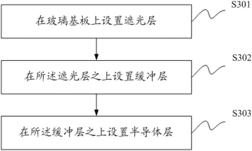
[0043] A method for preparing a thin film transistor provided in an embodiment of the present application, such as image 3 As shown, the method includes:

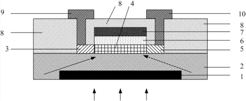
[0044] S301, setting a light-shielding layer on the glass substrate;

[0045] S302, setting a buffer layer on the light shielding layer;

[0046] S303, setting a semiconductor layer on the buffer layer;

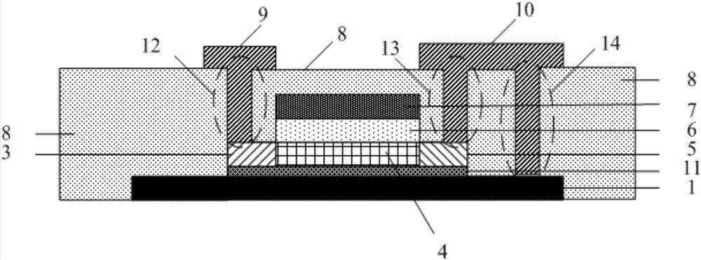
[0047] The semiconductor layer includes three regions: a channel region, a first conductorized region and a second conductorized region formed through conductorization treatment, and in a direction parallel to the semiconductor layer, the channel region is located on the Between the first conductorized region and the second conductorized region; wherein, the thickness of the buffer layer is such that the light incident on the buffer layer cannot affect the first conductorized region, the channel region and the Second conductorized area.

[0048] Preferably, setting the light-shielding layer on the glass substrate spec...


PUM


Abstract

The invention discloses a thin-film transistor, a preparation method thereof, an array substrate and a display panel, wherein the light shading effect of the channel region of the thin-film transistor is enhanced and the illumination stability of the thin-film transistor is therefore improved. The working stability of the thin-film transistor is enhanced. According to the embodiment of the invention, the thin-film transistor comprises a light-shading layer, a buffer layer positioned on the light-shading layer, and a semiconductor layer positioned on the buffer layer. The semiconductor layer comprises three partial regions, namely a first conductor region, a channel region and a second conductor region. In a direction parallel to the semiconductor layer, the channel region is positioned between the first conductor region and the second conductor region. The thickness of the buffer layer enables the incident light passing through the buffer layer not to influence the first conductor region, the channel region and the second conductor region.

Description

technical field [0001] The present application relates to the field of display technology, in particular to a thin film transistor and a manufacturing method thereof, an array substrate, and a display panel. Background technique [0002] The oxide thin film transistor (TFT) gate of the top gate structure does not overlap with the source and drain, so it has a small parasitic capacitance (Cgs), which can be applied to high resolution and high refresh rate, Large-size organic light-emitting diode (OLED) display products with narrow borders and low power consumption. However, since the oxide in the oxide TFT is sensitive to light, the electrical characteristics of the oxide in the channel region of the TFT will change under light. The shading of the channel area, the TFT is prone to a large threshold voltage (V TH ) drift, which exceeds the compensation range of the compensation circuit, causing problems such as afterimages on the display screen. Therefore, when making an oxi...

Claims


Application Information

Patent Timeline
Patent Type & Authority Applications(China)
IPC IPC(8): H01L29/786
CPCH01L29/78633H01L29/7869H01L29/66969H01L29/41733H01L29/78603
Inventor 王国英宋振
Owner BOE TECH GRP CO LTD
Why Eureka
Try Eureka