Photoresist stripping solution

A stripping solution and photoresist technology, used in optics, opto-mechanical equipment, photosensitive material processing, etc., can solve the problems of ineffective removal, weak degumming ability, limited use range, etc., and achieve long service life and degumming ability. Strong, large operation window effect

Inactive Publication Date: 2017-08-22
KUNSHAN SIGO MICROELECTRONICS MATERIALS
View PDF11 Cites 5 Cited by
  • Summary
  • Abstract
  • Description
  • Claims
  • Application Information

AI Technical Summary

Problems solved by technology

This type of photoresist stripping solution has weak degumming ability and can only be used to remove positive and negative photoresists with a thickness less than about 5 microns. For some photoresist residues that are highly hardened and crosslinked by photolithography processes, and Some polyacrylate and polyimide negative thick film photoresists cannot be removed effectively, which limits the scope of use

Method used


Image

  • Photoresist stripping solution
  • Photoresist stripping solution
  • Photoresist stripping solution

Examples


Embodiment Construction

[0013] The advantages of the present invention are further described below through specific examples, but the protection scope of the present invention is not limited only to the following examples.

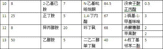
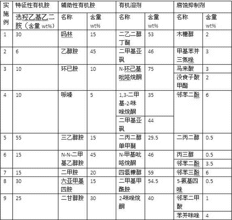
[0014] Table 1 The composition and content of cleaning solution of embodiment and comparative example

[0015]

[0016]

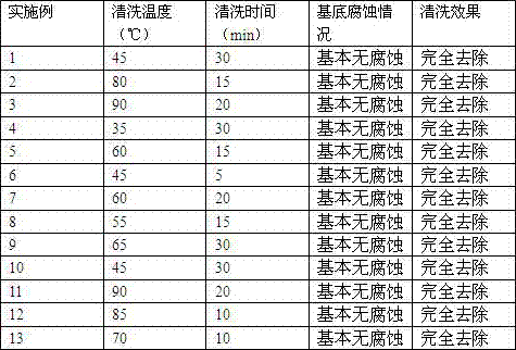
[0017] In order to further investigate the cleaning situation of this type of photoresist stripping solution, the present invention adopts the following technical means: the wafer that is about to be covered with thick film negative photoresist is cut into 3cm*3cm chips, respectively immersed in 100mL cleaning solution Soak at 30°C to 90°C for 3-30min, then rinse and dry with high-purity nitrogen. The cleaning effect of photoresist residues and the corrosion of the wafer substrate by the stripping solution are shown in Table 2

[0018]

[0019] It can be seen from Table 2 that the photoresist stripping solution of the present invention has a strong r...


PUM


Abstract

The invention relates to a photoresist stripping solution which is characterized by being prepared from organic amine, auxiliary organic amine, a polar organic solvent and a corrosion inhibitor. For solving the problem that an existing photoresist stripping solution operating window is small, the wafer substrate corrosivity is stronger and especially the capability of removing deeply hardened and cross-linked photoresist residues and a negative thick film photoresist is weak, the photoresist stripping solution which is strong in photoresist removal capability and large in operating window and does not corrode a wafer substrate is provided. The photoresist stripping solution can very effectively remove the photoresist and photoresist residues on LED chips and semiconductor wafers and especially has the strong capability of removing the deeply hardened and cross-linked photoresist residues and the negative thick film photoresist. In addition, the wafer substrate material is not corroded, the operating window is larger, and the service life is longer.

Description

technical field [0001] The invention relates to the field of chemical preparations, in particular to a photoresist stripping solution for removing photoresist residues on microelectronic substrates such as LEDs and semiconductor devices. Background technique [0002] In the usual manufacturing process of LED and semiconductor devices, photoresist is needed as an anti-mask for patterned transfer. After photolithography processes such as exposure, development, etching and patterned transfer are completed, photoresist residues need to be removed so that Proceed to the next process. This process requires complete removal of photoresist residues without etching any substrate. [0003] At present, the photoresists used in the photolithography process are mainly Novolic positive resists and polyacrylate negative resists, and the corresponding adhesive removers are mainly alkaline photoresist strippers. One type of alkaline photoresist stripping solution mainly contains strong ino...

Claims


Application Information

Patent Timeline
Patent Type & Authority Applications(China)
IPC IPC(8): G03F7/42
CPCG03F7/426
Inventor 刘江华
Owner KUNSHAN SIGO MICROELECTRONICS MATERIALS
Why Eureka
Try Eureka