Surface-treated copper foil for printed circuit board, copper-clad laminate for printed circuit board, and printed circuit board

A technology for printed circuit boards and copper clad laminates, which is applied in the secondary processing of printed circuits, printed circuits, and printed circuit manufacturing. , Excellent durability and high adhesion

Active Publication Date: 2017-08-29
FURUKAWA ELECTRIC CO LTD
View PDF6 Cites 7 Cited by
  • Summary
  • Abstract
  • Description
  • Claims
  • Application Information

AI Technical Summary

Problems solved by technology

At this time, since the resin penetrates to the roots of the roughened particles formed on the roughened surface of the copper foil, the larger the roughened particles, the deeper the irregularities transferred to the resin. The light of the resin substrate is easily scattered, and the light transmittance tends to be poor

Method used


Image

  • Surface-treated copper foil for printed circuit board, copper-clad laminate for printed circuit board, and printed circuit board
  • Surface-treated copper foil for printed circuit board, copper-clad laminate for printed circuit board, and printed circuit board
  • Surface-treated copper foil for printed circuit board, copper-clad laminate for printed circuit board, and printed circuit board

Examples


Embodiment

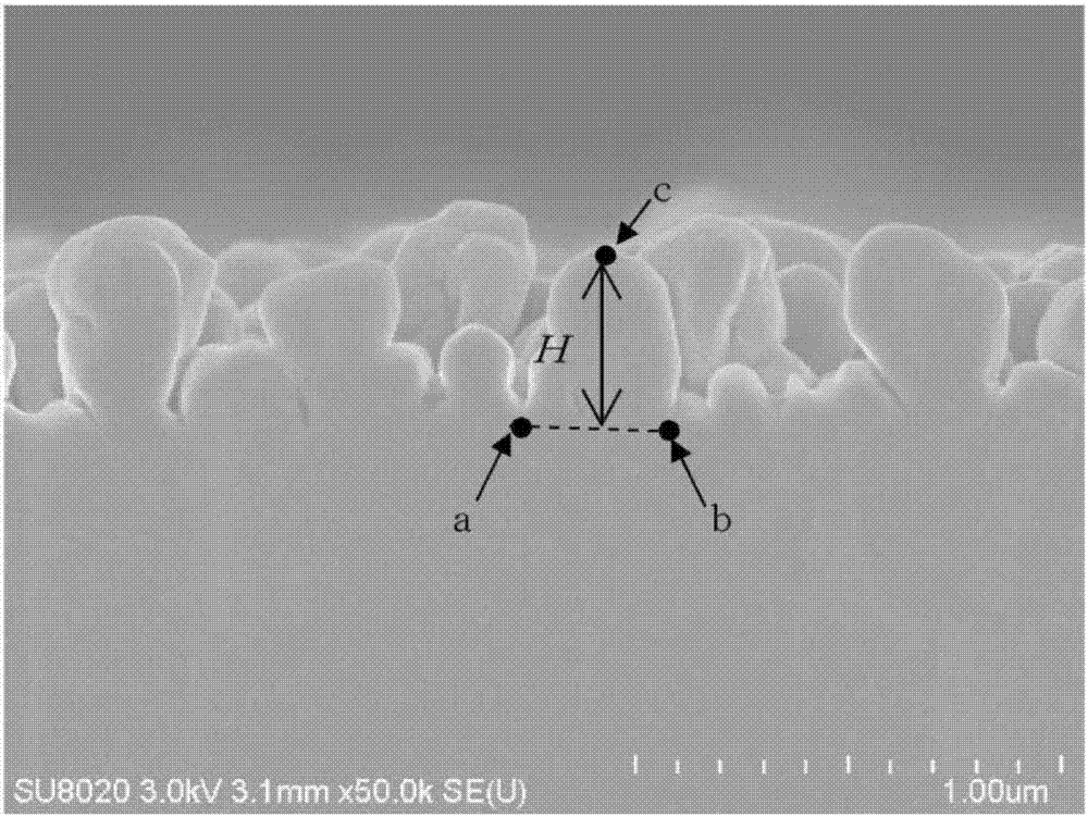
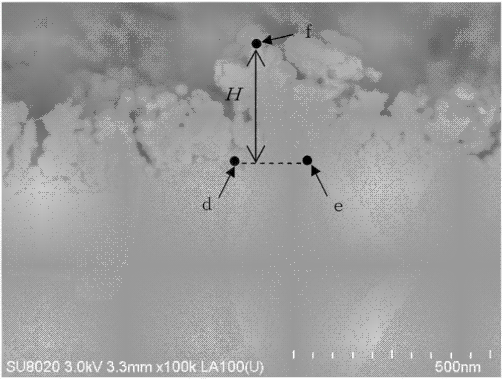
[0103] Hereinafter, the present invention will be described in more detail based on examples. In addition, the following is an example of the present invention, and in carrying out the present invention, various forms can be adopted as long as they do not deviate from the gist of the present invention.

[0104] [production of copper foil]

[0105] Electrolytic copper foil or rolled copper foil is used as the copper foil of the base material for roughening treatment.

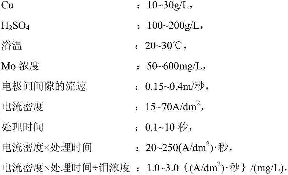
[0106] In Examples 1, 2, 4, 5, 7, 8, Comparative Examples 1 to 4, and 7, and Reference Example 1, an electrolytic copper foil having a thickness of 12 μm produced under the following conditions was used.

[0107]

[0108]

[0109] (additive)

[0110] 3-mercapto 1-propanesulfonate sodium: 2mg / L,

[0111] ·Hydroxyethyl cellulose: 10mg / L,

[0112] ·Low molecular weight glue (molecular weight: 3000): 50mg / L.

[0113] In Examples 3 and 6 and Comparative Examples 5 and 6, a commercially available 12 μm toughe...


PUM

PropertyMeasurementUnit
heightaaaaaaaaaa
heightaaaaaaaaaa
surface roughnessaaaaaaaaaa

Abstract

A surface-treated copper foil that is for a printed circuit board and that has a silane coupling agent layer on a surface on which roughened particles have been formed. The average height of the roughened particles on the silane-coupling-agent-layer surface is 0.05 [mu]m or more but less than 0.5 [mu]m, the BET surface area ratio of the of the silane-coupling-agent-layer surface is 1.2 or higher, and the micro-surface coefficient Cms of the silane-coupling-agent-layer surface is 2.0 or higher but less than 8.0.

Description

technical field [0001] The invention relates to a surface-treated copper foil for a printed circuit board. Moreover, this invention relates to the copper-clad laminated board for printed wiring boards which used this surface-treated copper foil for printed wiring boards, and a printed wiring board. Background technique [0002] In recent years, with the development of high-performance / high-function and networking of computers and information communication equipment, it is necessary to transmit and process large-capacity information at a higher speed. Therefore, the transmitted signal tends to be more high-frequency, and the printed circuit board is required to suppress the transmission loss of high-frequency signals. In the production of printed wiring boards, copper foil is usually laminated on an insulating base material (resin base material), heated, pressurized, and bonded to produce a copper-clad laminate, and the copper-clad laminate is used Laminates to form conduct...

Claims


Application Information

Patent Timeline
Patent Type & Authority Applications(China)
IPC IPC(8): C25D7/06B32B15/04B32B15/08C25D5/16C25D5/48H05K1/09H05K3/38
CPCB32B15/04B32B15/08C25D5/48C25D7/06H05K1/09H05K3/38C25D5/627C25D5/605H05K3/384H05K3/389
Inventor 斋藤贵广绘面健
Owner FURUKAWA ELECTRIC CO LTD
Why Eureka
Try Eureka