Perfect absorber
A perfect absorption, cylindrical technology, applied in optical components, optics, instruments, etc., can solve problems such as poor absorption effect
- Summary
- Abstract
- Description
- Claims
- Application Information
AI Technical Summary
Problems solved by technology
Method used
Image
Examples
Embodiment Construction
[0013] In order to make the technical problems, technical solutions and beneficial effects to be solved by the present invention clearer, the present invention will be further described in detail below in conjunction with the embodiments. It should be understood that the specific embodiments described here are only used to explain the present invention, not to limit the present invention.
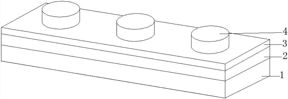
[0014] Such as figure 1 , 2 , 3, the embodiment of the present invention provides a perfect absorbent body. The perfect absorber includes a substrate layer 1 with two opposite surfaces, a metal layer 2 and a dielectric layer 3 stacked in sequence from one surface of the substrate layer 1 outward, and a metal layer stacked on the surface of the dielectric layer 3 Metal Nanoarray 4;
[0015] Wherein, the metal nanoarray 4 is any one of a cylinder array, a 3D spiral array, a prism array, and a regular prism array.
[0016] In any embodiment, the substrate 1 is any one of quartz, silicon wa...
PUM
| Property | Measurement | Unit |
|---|---|---|
| Cycle | aaaaa | aaaaa |
| Height | aaaaa | aaaaa |
| Diameter | aaaaa | aaaaa |
Abstract
Description
Claims
Application Information


