A device structure suitable for monochromatic LED wafer level packaging

A device structure, wafer-level technology, applied in the direction of electrical components, semiconductor devices, circuits, etc., can solve the problems of poor heat dissipation, light side leakage of monochromatic LED devices, and low light output efficiency, so as to increase the contact area, improve the Conducive to the effect of uniform expansion and improved optical power

Active Publication Date: 2019-12-27
SHANGHAI XINYUANJI SEMICON TECH
View PDF3 Cites 0 Cited by
  • Summary
  • Abstract
  • Description
  • Claims
  • Application Information

AI Technical Summary

Problems solved by technology

[0007] In view of the shortcomings of the prior art described above, the purpose of the present invention is to provide a device structure suitable for monochromatic LED wafer level packaging, which is used to solve the problem of light side leakage, poor heat dissipation, Problems such as low light extraction efficiency

Method used


Image

  • A device structure suitable for monochromatic LED wafer level packaging
  • A device structure suitable for monochromatic LED wafer level packaging
  • A device structure suitable for monochromatic LED wafer level packaging

Examples


Embodiment Construction

[0059] Embodiments of the present invention are described below through specific examples, and those skilled in the art can easily understand other advantages and effects of the present invention from the content disclosed in this specification. The present invention can also be implemented or applied through other different specific implementation modes, and various modifications or changes can be made to the details in this specification based on different viewpoints and applications without departing from the spirit of the present invention.

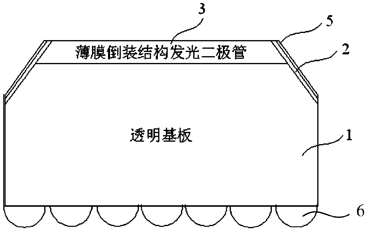
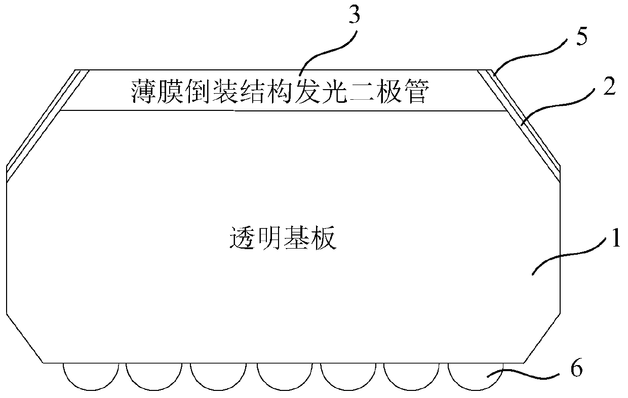
[0060] Please refer to attached picture. It should be noted that the diagrams provided in this embodiment are only schematically illustrating the basic idea of ​​the present invention, and only the components related to the present invention are shown in the diagrams rather than the number, shape and shape of the components in actual implementation. Dimensional drawing, the type, quantity and proportion of each component can be change...


PUM


Abstract

The invention provides a device structure suitable for monochromatic LED wafer-level package. The device structure at least includes a transparent substrate, a light emitting diode chip of a thin-film flip-chip structure bonded to the upper surface of the transparent substrate, and first reflectors and passivation layers which cover the sides of the transparent substrate and the light-emitting diode chip of a thin-film flip-chip structure in turn. The transparent substrate is machined into a trapezoidal structure facilitating light output. The lower surface of the transparent substrate is provided with a structure facilitating light output, such as a micro lens array structure or a V groove structure. The surface of an N-type semiconductor layer of the light emitting diode chip of a thin-film flip-chip structure is provided with a micro tapered coarse structure. The coarse structure is bonded to the upper surface of the transparent substrate, so that light emitted by the LED chip can enter the transparent substrate easily. The first reflectors and a reflector on the surface of a P-type layer of the thin-film flip chip form a trapezoidal reflector cup, which enables monochromatic light emitted by the chip to enter the transparent substrate from the surface of the N-type semiconductor layer completely and then go out to the air from the lower surface with a structure facilitating light output of the transparent substrate. By using a transparent substrate material with moderate refractive index, the total reflection of light directly from gallium nitride to the air is reduced greatly, and the light output efficiency of devices is increased.

Description

technical field [0001] The invention relates to the technical field of LEDs, in particular to a device structure suitable for monochrome LED wafer-level packaging. Background technique [0002] Light-emitting diodes have the advantages of small size, high efficiency and long life, and are widely used in traffic indication, outdoor full-color display and other fields. In particular, the use of high-power light-emitting diodes may realize semiconductor solid-state lighting, which has caused a revolution in the history of human lighting, and has gradually become a research hotspot in the field of electronics. The light extraction efficiency of LED refers to the ratio of the available photons incident to the device and the photons generated by electron-hole recombination in the active area of ​​the epitaxial wafer. In traditional LED devices, due to factors such as substrate absorption, electrode blocking, and total reflection of the light-emitting surface, the light extraction...

Claims


Application Information

Patent Timeline
Patent Type & Authority Patents(China)
IPC IPC(8): H01L33/02H01L33/46H01L33/22
CPCH01L33/02H01L33/22H01L33/46
Inventor 郝茂盛张楠袁根如
Owner SHANGHAI XINYUANJI SEMICON TECH
Why Eureka
Try Eureka