Testability design circuit applied to anti-fuse FPGA (Field-Programmable Gate Array)

A technology for designing circuits and programming logic, which is applied in the field of microelectronics and can solve problems such as circuit programming and functional testing.

Inactive Publication Date: 2017-09-05
58TH RES INST OF CETC
View PDF5 Cites 4 Cited by
  • Summary
  • Abstract
  • Description
  • Claims
  • Application Information

AI Technical Summary

Problems solved by technology

However, antifuse is not as erasable as static random access memory (English: Static Random Access Memory, referred to as: SRAM) or Flash. Therefore, antifuse FPGA can only be programmed once, and the programming is done by the user. before end use
[0005] One of the difficulties of the anti-fuse FPGA circuit is the circuit test. Since the FPGA circuit does not have any functions without configuration, and the anti-fuse FPGA can only be programmed once, it cannot be programmed in the test phase like SRAM or Flash FPGA. function to test

Method used


Image

  • Testability design circuit applied to anti-fuse FPGA (Field-Programmable Gate Array)

Examples


Embodiment Construction

[0020] Reference will now be made in detail to the exemplary embodiments, examples of which are illustrated in the accompanying drawings. When the following description refers to the accompanying drawings, the same numerals in different drawings refer to the same or similar elements unless otherwise indicated. The implementations described in the following exemplary examples do not represent all implementations consistent with the present invention. Rather, they are merely examples of apparatuses and methods consistent with aspects of the invention as recited in the appended claims. The "connection" mentioned in the article is an electrical connection, which can be a direct electrical connection or an indirect electrical connection; the "at least one" mentioned in the article means one, two or more than two; At least two" means two or more.

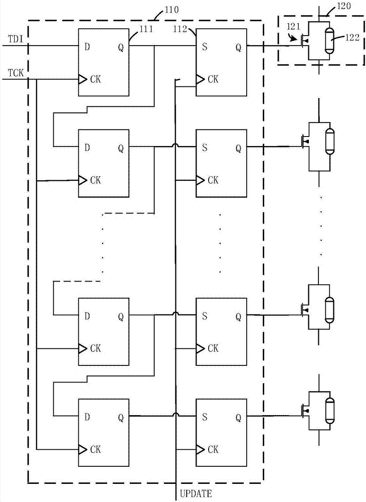
[0021] figure 1 A structural diagram of a design-for-test circuit suitable for an anti-fuse FPGA provided for an embodiment of the pr...


PUM


Abstract

The invention provides a testability design circuit applied to an anti-fuse FPGA (Field-Programmable Gate Array), and belongs to the technical field of micro-electronics. The testability design circuit comprises a control circuit and at least one switch completed circuit; each switch completed circuit includes an anti-fuse and a testing switch tube arranged in parallel connection; the testing switch tube is controlled by the control circuit to be opened or closed; after the testing switch tube is opened, the anti-fuse is in a short circuit; and after the testing switch tube is closed, the anti-fuse is enabled. According to the testability design circuit provided by the invention, by enabling the anti-fuse to connect one testing switch tube in parallel, the control circuit can be enabled to selectively control the opening of the testing switch tube in the switch completed circuit, and thus, the anti-fuse corresponding to a circuit that needs to be tested is guaranteed to be in the short circuit in a testing stage; and in a service stage, the testing switch tube is closed, the anti-fuse is enabled, and the closed testing switch tube does not affect signal transmission and also does not bring extra power consumption.

Description

technical field [0001] The invention belongs to the technical field of microelectronics and relates to a design-for-test structure applicable to an anti-fuse programmable logic gate array (English: Field-Programmable Gate Arra, FPGA for short). Background technique [0002] The anti-fuse FPGA chip is an FPGA circuit that uses a special device such as an anti-fuse as a programming control unit, and the anti-fuse acts as a pass switch in the circuit. [0003] The antifuse is embedded between the top layer and the second top layer of metal. The antifuse dielectric exists in the form of a similar via. Since the antifuse dielectric layer conducts poorly, the antifuse via connection is normally open. . However, after high-voltage programming, the antifuse medium will be broken down, and at this time, the antifuse medium will dissolve with the metal medium to conduct. In this way, before programming, the antifuse via is in an open state, and after programming, the antifuse via is...

Claims


Application Information

Patent Timeline
Patent Type & Authority Applications(China)
IPC IPC(8): H03K19/177G01R31/3185G01R31/28
CPCG01R31/2851G01R31/318519H03K19/17708
Inventor 曹靓封晴隽扬马金龙王栋
Owner 58TH RES INST OF CETC
Why Eureka
Try Eureka