Measurement method of electron microscopic image line width and roughness

A technology of line width and electron microscopy, applied in the direction of electric/magnetic roughness/irregularity measurement, electromagnetic measuring device, measuring device, etc., can solve the problem of only analyzing limited data points and measuring line width and roughness Large volume, measurement error and other problems, to achieve the effect of reducing limitations, reducing the influence of background pixels, and accurate boundary positioning

Active Publication Date: 2017-09-08
INST OF MICROELECTRONICS CHINESE ACAD OF SCI
View PDF5 Cites 6 Cited by
  • Summary
  • Abstract
  • Description
  • Claims
  • Application Information

AI Technical Summary

Problems solved by technology

[0004] The embodiment of the present application provides a method for measuring the line width and roughness of electron microscopic images, which solves the problem of large workload in measuring line width and roughness in the prior art, measurement errors caused by human intervention, and limited analysis. data point problem

Method used


Image

  • Measurement method of electron microscopic image line width and roughness
  • Measurement method of electron microscopic image line width and roughness
  • Measurement method of electron microscopic image line width and roughness

Examples


Embodiment 1

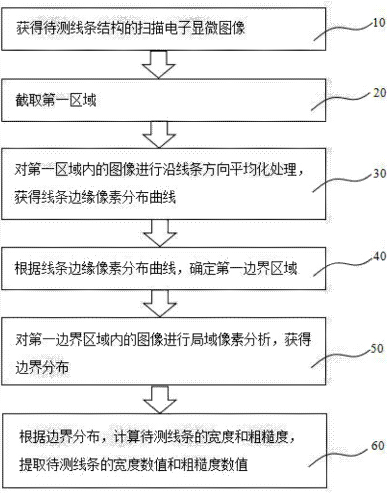
[0049] This embodiment provides a method for measuring line width and roughness of an electron microscopic image, such as figure 1 shown, including:

[0050] Step 10: Obtain a scanning electron microscopic image of the line structure to be tested.

[0051] The line structure to be tested may be a photolithography pattern obtained after a photolithography process. The photolithography process is to form a pattern on the photoresist, and the pattern is further used as a mask layer for etching. The structure of the side lines to be etched can also be obtained by etching the layer to be etched to obtain an intermediate pattern or target pattern, and the layer to be etched can be any required material layer, substrate, dielectric material layer or metal layer, etc. For the material layer to be etched, the etching process can be wet etching or photolithography etching. The line structure to be tested may be a sliced ​​line pattern. The line structure to be measured may also be a...


PUM


Abstract

The present invention belongs to the scanning electron microscopic measurement technology field, and discloses a measurement method of the electron microscopic image line width and roughness. The method comprises the steps of obtaining a scanning electron microscopic image of a to-be-measured line structure; intercepting a first area; processing averagely along a line direction, and obtaining a line edge pixel distribution curve; according to the line edge pixel distribution curve, determining a first boundary area; analyzing the local pixels, and obtaining the boundary distribution; according to the boundary distribution, calculating the width and the roughness of a to-be-measured line, and extracting the width and roughness numerical values of the to-be-measured line. The measurement method of the present invention solves the problems in the prior art that the workload of measuring the line width and roughness is larger, a measurement error caused by the human intervention exists, and a limited number of data points only can be analyzed, and realizes the technical effects of improving the measurement accuracy and reliability, saving the actual measurement time and cost of the engineers.

Description

technical field [0001] The invention relates to the technical field of scanning electron microscopic measurement, in particular to a method for measuring line width and roughness of an electron microscopic image. Background technique [0002] In the fields of microelectronics, optoelectronics, MEMS, etc., accurate measurement of line width and roughness is a very important application. Especially for some cases, the micro-nano device structure contains a very serious background electron beam intensity distribution, for example, the existence of patterns in the front layer has a great influence on the electron beam imaging, or the electron beam imaging of the section after slicing and the evaluation along the height The distribution of the background electron beam is seriously affected by the height position when the width of the line is measured in the direction of the line. These phenomena all make there are serious defects in the measurement of the line width. [0003] Wh...

Claims


Application Information

Patent Timeline
Patent Type & Authority Applications(China)
IPC IPC(8): G01B7/02G01B7/34
CPCG01B7/02G01B7/34
Inventor 张利斌韦亚一
Owner INST OF MICROELECTRONICS CHINESE ACAD OF SCI
Why Eureka
Try Eureka