Method for rapidly cutting silicon wafers with electroplating diamond wire with ultrahigh efficiency

A fast cutting and ultra-efficient technology, used in fine work equipment, work accessories, stone processing equipment, etc., can solve the problems of low efficiency of electroplating diamond wire cutting silicon wafers, and achieve the goal of reducing the demand for new lines and reducing fatigue. Effect

Active Publication Date: 2017-09-15
杨凌美畅新材料股份有限公司
View PDF9 Cites 21 Cited by
  • Summary
  • Abstract
  • Description
  • Claims
  • Application Information

AI Technical Summary

Problems solved by technology

[0008] Aiming at the problem of low efficiency of electroplating diamond wire cutting silicon wafers in the prior art, th

Method used


Image

  • Method for rapidly cutting silicon wafers with electroplating diamond wire with ultrahigh efficiency
  • Method for rapidly cutting silicon wafers with electroplating diamond wire with ultrahigh efficiency
  • Method for rapidly cutting silicon wafers with electroplating diamond wire with ultrahigh efficiency

Examples


Embodiment 2

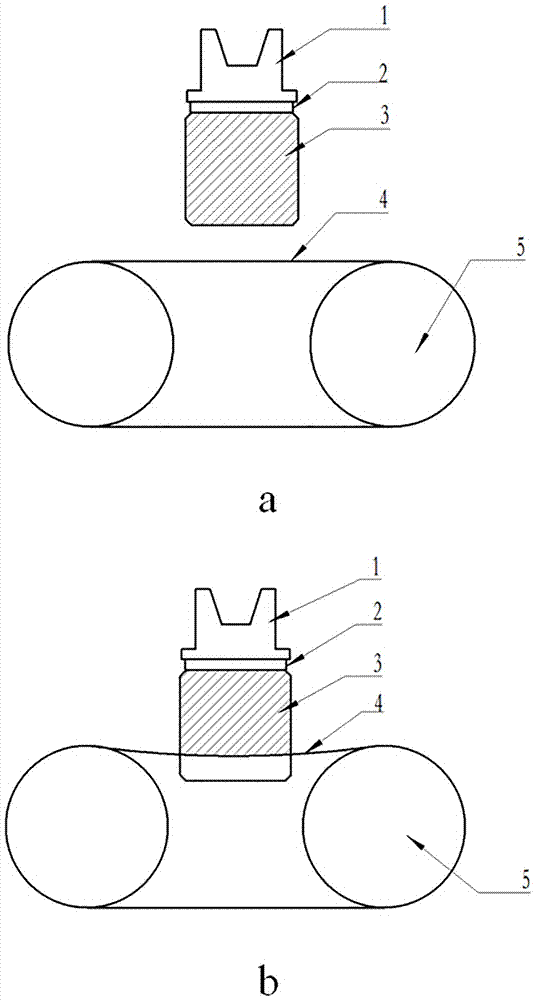
[0057] A method for quickly cutting silicon wafers with an ultra-efficient electroplating diamond wire, comprising the following steps: (1) sticking sticks, (2) loading, (3) preparing cutting fluid, (4) cutting, (5) unloading, (6) ) degumming, cleaning, (7) detection, packaging;

[0058] Bond the dovetail 1 and the resin plate 2, the resin plate 2 and the silicon rod 3 with epoxy resin AB glue; put the bonded whole on the loading and unloading tool through the dovetail, and send it to the slicer; cut the purchased high-tech Liquid, Defeng defoamer, and water are mixed evenly according to the mass ratio of 1:1:300, then poured into the cutting fluid tank and set aside.

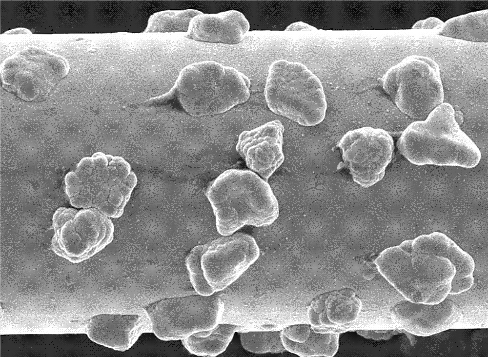
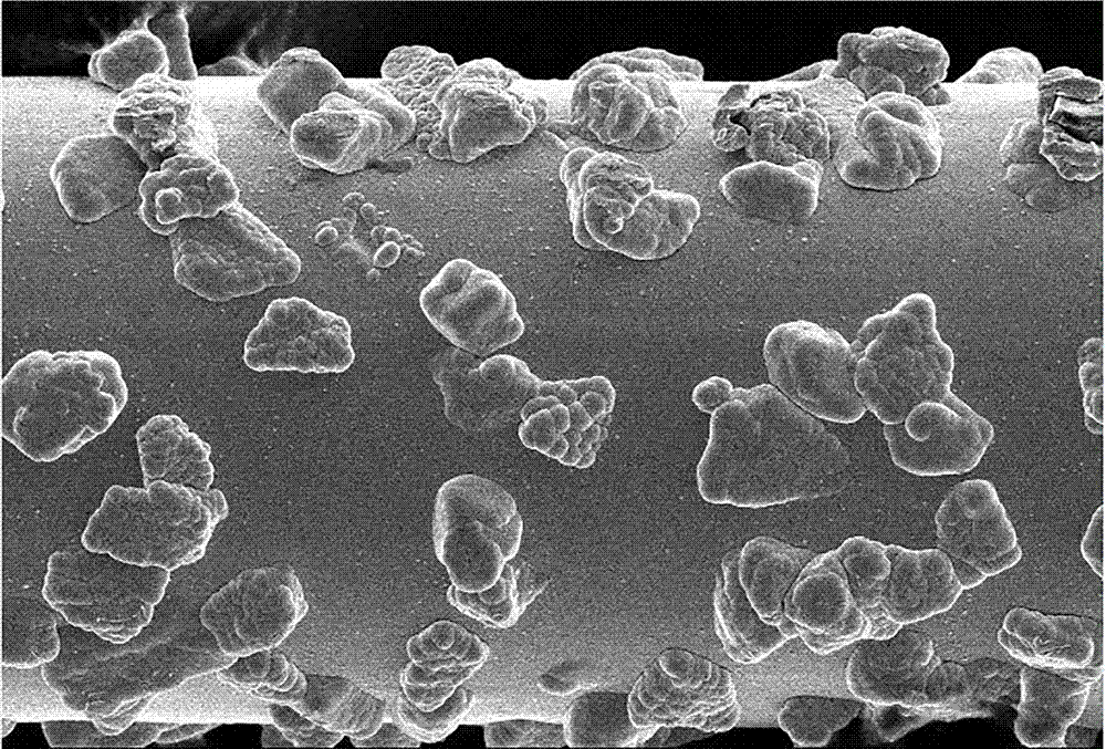
[0059] image 3 For the electron micrograph of the electroplated diamond wire used in the present embodiment, the electroplated diamond wire with a diameter of 70um is used as the cutting wire in the present embodiment, as shown in image 3 As shown, the density of diamond particles on the electroplated diamo...

Embodiment 3

[0070] A method for quickly cutting silicon wafers with an ultra-efficient electroplating diamond wire, comprising the following steps: (1) sticking sticks, (2) loading, (3) preparing cutting fluid, (4) cutting, (5) unloading, (6) ) degumming, cleaning, (7) detection, packaging;

[0071] Bond the dovetail 1 and the resin plate 2, the resin plate 2 and the silicon rod 3 with epoxy resin AB glue; put the bonded whole on the loading and unloading tool through the dovetail, and send it to the slicer; cut the purchased high-tech Liquid, Defeng defoamer, and water are mixed evenly according to the mass ratio of 1:1:300, then poured into the cutting fluid tank and set aside.

[0072] Such as image 3 Shown is the electron micrograph of the electroplated diamond wire used in the present embodiment, adopting the electroplated diamond wire with a diameter of 70um as the cutting wire in the present embodiment, as image 3 As shown, the density of diamond particles on the electroplated di...


PUM

PropertyMeasurementUnit
Thicknessaaaaaaaaaa
Thicknessaaaaaaaaaa
Diameteraaaaaaaaaa

Abstract

The invention provides a method for rapidly cutting silicon wafers with an electroplating diamond wire with ultrahigh efficiency. The method includes the following steps that firstly, bar sticking is conducted; secondly, feeding is conducted; thirdly, a cutting solution is prepared; fourthly, cutting is conducted; fifthly, discharging is conducted; sixthly, degumming and cleaning are conducted; and seventhly, checking and packaging are conducted. According to cutting, a cutting rack drives a silicon bar to move towards the electroplating diamond wire, and meanwhile a main roller drives an electroplating diamond wire net to conduct reciprocating movement to achieve cutting; in the cutting process, the linear speed of the electroplating diamond wire ranges from 1300 m/min to 1500 m/min, the workpiece cutting speed ranges from 1 mm/min to 4.5 mm/min, and the thickness of a diamond particle coating on the electroplating diamond wire ranges from 3 microns to 5 microns; and in the cutting process, the manner of conducting forward feeding firstly and backward feeding secondly is adopted in the electroplating diamond wire, and before each workpiece is machined, the 3 km-5 km electroplating diamond wire is fed to a wire collecting wheel. By means of the cutting method, 8.4 inch and 650 mm crystalline silicon bars can be smoothly cut within 1 h, and the problem that in the prior art the efficiency for cutting silicon wafers with electroplating diamond wire is low is solved.

Description

technical field [0001] The invention relates to a method for multi-wire cutting solar-grade silicon wafers, in particular to a method for rapidly cutting silicon wafers with ultra-high-efficiency electroplating diamond wires. Background technique [0002] Solar energy is a renewable clean energy, and its application fields are becoming more and more extensive. Photovoltaic power generation is one of the most important fields. According to the principle of photovoltaic effect, solar cells are used to directly convert solar energy into electrical energy. Silicon wafers are an important part of solar cells. At present, almost all silicon wafer preparation processes use a multi-wire cutting method to cut crystalline silicon rods into silicon wafers of required thickness. Multi-wire cutting is mainly divided into two types: (1) Free abrasive cutting, that is, using fine wire steel wire to drive SiC slurry with a particle size of 8-20um to realize grinding and cutting of crystalli...

Claims


Application Information

Patent Timeline
IPC IPC(8): B28D5/04B28D7/02B28D7/04
CPCB28D5/0076B28D5/0082B28D5/042
Inventor 曲东升王新平曹民博
Owner 杨凌美畅新材料股份有限公司
Why Eureka
Try Eureka