
Method and device for growing multilayer heterojunctions through CVD

A technology of heterojunction and growth chamber, applied in coating, metal material coating process, gaseous chemical plating, etc., can solve the problems of difficulty in growing the second layer of heterojunction material, loss of catalytic effect, etc.

Active Publication Date: 2017-09-15
UNIV OF SCI & TECH OF CHINA
View PDF6 Cites 4 Cited by
  • Summary
  • Abstract
  • Description
  • Claims
  • Application Information

AI Technical Summary

Problems solved by technology

But after growing the first layer of material, the substrate is covered with material, which loses its catalytic effect, which makes it very difficult to grow the second layer of heterojunction material.

Method used


Image

  • Method and device for growing multilayer heterojunctions through CVD
  • Method and device for growing multilayer heterojunctions through CVD

Examples


Embodiment 1

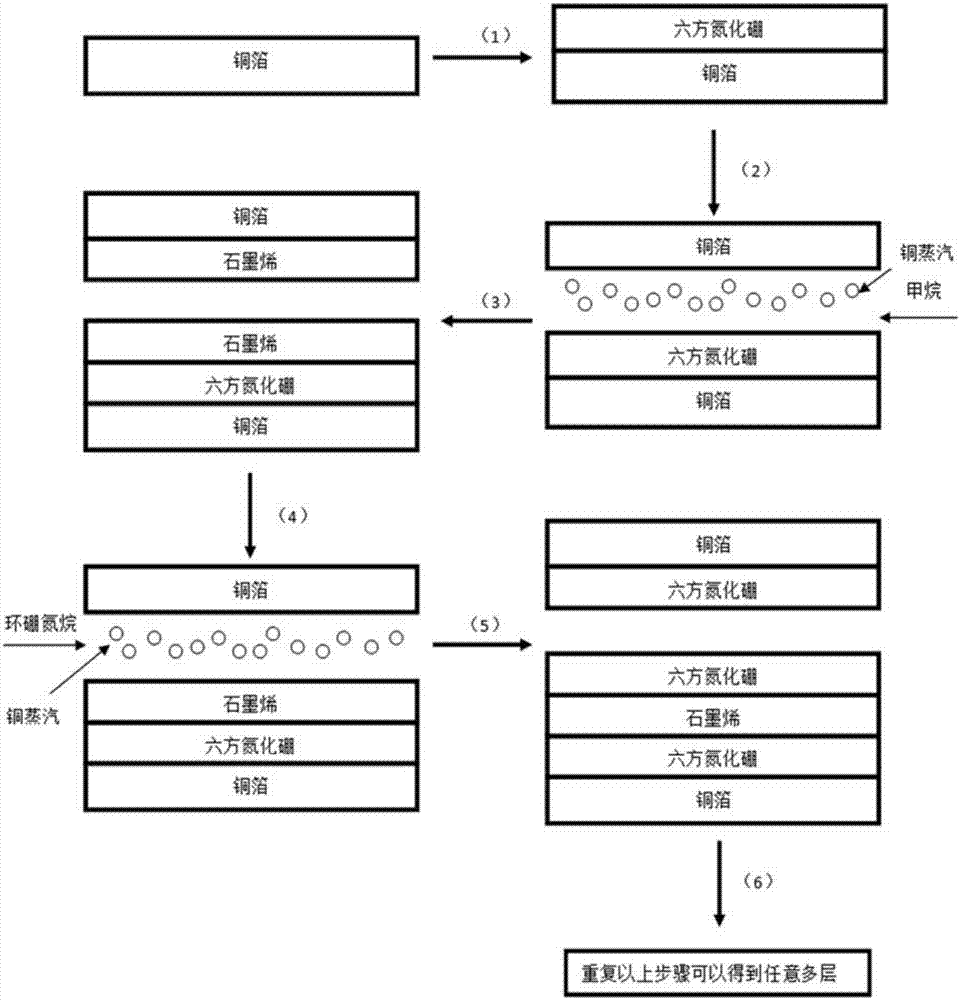
[0046] The flow chart of growing multilayer two-dimensional material heterojunction is attached figure 1 Shown: First, the base copper foil is loaded into the CVD growth chamber, the chamber is evacuated to a high vacuum, and the temperature is raised to a growth temperature of 1000°C. Because the cold wall system is used, the high temperature area will only be limited to a small area. Such a cold wall system has a good effect of suppressing dust pollution. After the temperature is raised to the growth temperature, an annealing process is performed for 2 hours. Then borazine is introduced to grow the first layer of hexagonal boron nitride on the base copper foil, and the growth time is about 40 minutes. When growing the first layer of material, the base copper can completely act as a catalyst, and there is no need to introduce suspended copper foil. After the growth of the first layer is completed, the base copper foil has lost the function of catalyst because it is complet...


PUM

PropertyMeasurementUnit
thicknessaaaaaaaaaa

Abstract

The invention provides a method and device for growing multilayer heterojunctions through CVD. According to the method, a CVD device is firstly used for growing a hexagonal boron nitride thin film on copper foil; and through a transmission device in the CVD device, new copper foil is moved to a high temperature growing zone for catalyzing carbon source for growing a graphene thin film. The above processes are repeatedly executed, and any multilayer boron nitride / graphene heterojunctions are obtained.

Description

technical field [0001] The invention relates to the technical field of nanomaterial preparation and chemical equipment, in particular to a method and device for preparing a multilayer two-dimensional material heterojunction. Background technique [0002] Graphene, as the hottest two-dimensional material in recent years, has been researched on it for more than ten years since it was successfully peeled off. Graphene is a carbon atom with sp 2 The honeycomb planar film formed by hybridization has many excellent characteristics, such as ultra-high electron mobility, ultra-high tensile strength and elastic modulus, ultra-high electrothermal performance, and near transparency. However, research in recent years has found that for a single graphene material, its application range is too narrow. If it can be combined with other materials, many novel phenomena will appear. [0003] As "white graphene", hexagonal boron nitride has attracted the attention of many research groups in r...

Claims


Application Information

Patent Timeline
Patent Type & Authority Applications(China)
IPC IPC(8): C23C16/26C23C16/34C23C16/44
CPCC23C16/26C23C16/342C23C16/44
Inventor 郭国平杨晖李海欧曹刚肖明郭光灿
Owner UNIV OF SCI & TECH OF CHINA
Learn More