Substrate annealing device

An annealing device and substrate technology, applied in the manufacture of electrical components, circuits, semiconductor/solid-state devices, etc., can solve the problems of high cost and low processing efficiency of laser annealing process, so as to improve the service life, increase the number of transmission and processing, and improve the The effect of efficiency

Active Publication Date: 2017-09-15
KUNSHAN GO VISIONOX OPTO ELECTRONICS CO LTD
View PDF13 Cites 7 Cited by
  • Summary
  • Abstract
  • Description
  • Claims
  • Application Information

AI Technical Summary

Problems solved by technology

[0004] Therefore, the technical problem to be solved by the present invention is to overcome the defects of low processing efficiency and high cost of the laser annealing process in the prior art, and a laser annealing device for amorphous silicon thin films is provided for this purpose

Method used


Image

  • Substrate annealing device
  • Substrate annealing device
  • Substrate annealing device

Examples


Embodiment 1

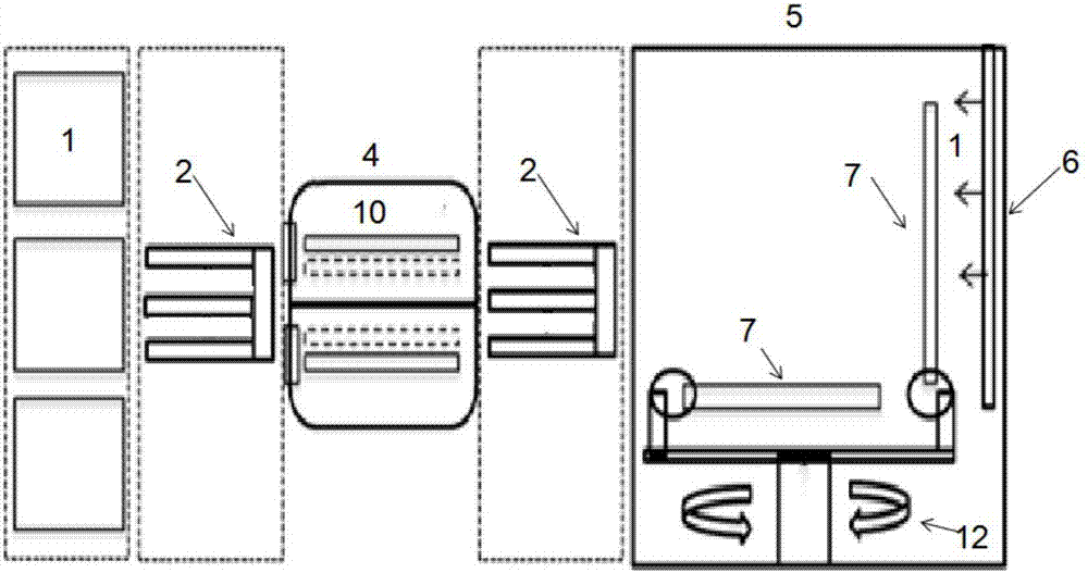
[0035] Such as figure 1 Shown is a substrate annealing device of the present invention, which mainly includes: a preheating chamber 4 and an annealing chamber 5 . The preheating chamber 4 is arranged upstream of the annealing chamber 5 , and the substrate 1 enters the preheating chamber 4 through the manipulator 2 . A heater is arranged in the preheating chamber 4, and the substrate 1 is preheated by the heater, wherein the heating temperature in the preheating chamber 4 ranges from 0°C to 600°C. After the preheating is completed, the substrate 1 is transferred to the annealing chamber 5 by the manipulator 2 for annealing treatment.

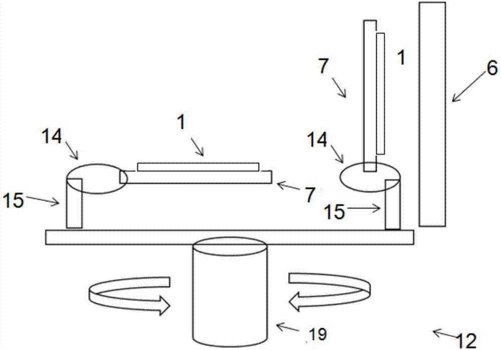
[0036]The annealing chamber 5 in this embodiment is provided with a laser annealing device 6 and a rotating device 12 , wherein the laser annealing device 6 is used for annealing the surface of the substrate 1 . Such as image 3 As shown, the rotating device 12 in this embodiment is provided with a plurality of irradiation positions 15 for fix...


PUM

PropertyMeasurementUnit
The average thicknessaaaaaaaaaa

Abstract

The invention discloses a substrate annealing device, comprising an annealing chamber, wherein a laser annealing device is arranged in the annealing chamber and is used for annealing surfaces of substrates; and the annealing chamber is equipped with a plurality of irradiation positions for fixing the substrates and the at least one laser annealing device for irradiating the substrates at the irradiation positions. According to the laser annealing device provided by the invention, an occupation space is saved, so the transmitting and processing number of the substrates is improved in the same space; and a plurality of transmitting chambers, preheating chambers and annealing chambers can be set, so efficient annealing can be realized, and the laser annealing productivity is improved.

Description

technical field [0001] The invention relates to the field of display technology, in particular to a substrate annealing device. Background technique [0002] With the development of display technology, active-matrix organic light emitting diode (AMOLED) panels are widely used. OLED has the advantages of high contrast, wide viewing angle, low power consumption, and small size. Based on the AMOLED panel, a technology called Low Temperature Poly-Silicon (LTPS) came into being. At present, LTPS technology now uses chemical vapor deposition to deposit a buffer layer on a glass substrate; then an amorphous silicon layer is deposited on the buffer layer, and the amorphous silicon layer is converted into a polysilicon layer by laser annealing equipment. [0003] In the prior art, an excimer laser is used to uniformly irradiate the amorphous silicon layer on the substrate, so that the amorphous silicon layer is melted at high temperature, and then recrystallized to form a polysilico...

Claims


Application Information

Patent Timeline
IPC IPC(8): H01L21/67
CPCH01L21/67115
Inventor 杨依辉
Owner KUNSHAN GO VISIONOX OPTO ELECTRONICS CO LTD
Why Eureka
Try Eureka