Array substrate and manufacturing method therefor and display apparatus

An array substrate and array arrangement technology, applied in semiconductor/solid-state device manufacturing, electrical components, electric solid-state devices, etc., can solve the problems of cumbersome process, low production efficiency, and increase driving thin film transistors, etc., and achieve simple manufacturing process and high production efficiency High Efficiency, Increased Subthreshold Swing Effect

Active Publication Date: 2017-09-15
WUHAN CHINA STAR OPTOELECTRONICS TECH CO LTD
View PDF6 Cites 9 Cited by
  • Summary
  • Abstract
  • Description
  • Claims
  • Application Information

AI Technical Summary

Problems solved by technology

In this manufacturing method, it is necessary to form two layers of gate insulating layers to increase the subthreshold swing of the driving thin film transistor T2, and the process is cumbersome and the manufacturing efficiency is low.

Method used


Image

  • Array substrate and manufacturing method therefor and display apparatus
  • Array substrate and manufacturing method therefor and display apparatus
  • Array substrate and manufacturing method therefor and display apparatus

Examples


Embodiment Construction

[0057] The implementation of the present invention will be described in detail below in conjunction with the accompanying drawings and examples, so as to fully understand and implement the process of how to apply technical means to solve technical problems and achieve technical effects in the present invention. It should be noted that, as long as there is no conflict, each embodiment and each feature in each embodiment of the present invention can be combined with each other, and the formed technical solutions are all within the protection scope of the present invention.

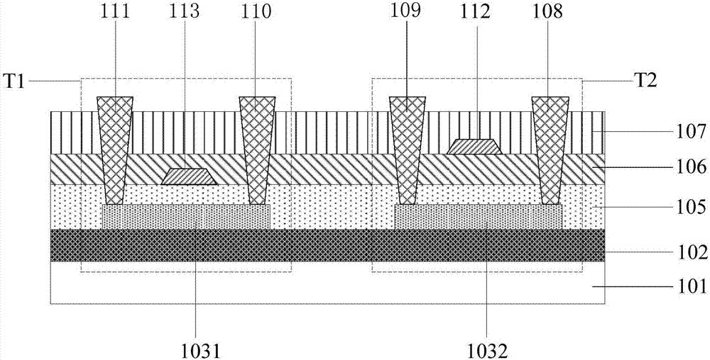
[0058] In order to solve the problems of cumbersome manufacturing process and low manufacturing efficiency of the double-layer gate insulating layer used to increase the sub-threshold swing of the driving thin film transistor in the prior art, the present invention provides an array using a layer of gate insulating layer substrate. The array substrate includes a plurality of pixel units arranged in an array,...


PUM


Abstract

The invention provides an array substrate and a manufacturing method therefor and a display apparatus. Each of a switching thin film transistor and a driving thin film transistor in the array substrate comprises an active layer, a planarization gate insulating layer and a gate separately; the active layers are both arranged on a substrate; the thickness of the active layer of the switching thin film transistor is greater than that of the active layer of the driving thin film transistor; the switching thin film transistor and the driving thin film transistor share the planarization gate insulating layer, and are arranged on the active layers and the exposed substrate; and the gate of the switching thin film transistor and the gate of the driving thin film transistor are arranged on the planarization gate insulating layer. The process is simple and the manufacturing efficiency of the array substrate can be improved.

Description

technical field [0001] The present invention belongs to the field of display technology, and in particular, relates to an array substrate, a manufacturing method thereof, and a display device. Background technique [0002] The flat panel display device has many advantages such as thin body, power saving, and no radiation, so it has been widely used. Flat panel display devices mainly include Liquid Crystal Display (LCD for short) and Organic Light Emitting Diode (OLED for short) displays. OLED has the following excellent characteristics: ① self-illumination, no backlight required; ② high contrast; ③ thin thickness; ④ wide viewing angle; ⑤ fast response; ⑥ can be used for flexible panels; The manufacturing process is simple, so it is regarded as a new application technology for the next generation of flat panel displays. [0003] Organic light emitting diode displays can be divided into passive matrix organic light emitting diode displays (Passive Matrix Organic Light Emitti...

Claims


Application Information

Patent Timeline
IPC IPC(8): H01L27/12H01L27/32H01L29/423H01L21/77
CPCH01L27/1233H01L27/127H01L27/1288H01L29/42364H10K59/12
Inventor 邢磊
Owner WUHAN CHINA STAR OPTOELECTRONICS TECH CO LTD
Why Eureka
Try Eureka