Display panel and display device

A display panel and substrate technology, applied in nonlinear optics, instruments, optics, etc., can solve problems such as light crosstalk

Active Publication Date: 2017-09-29
SHENZHEN CHINA STAR OPTOELECTRONICS TECH CO LTD
View PDF5 Cites 12 Cited by
  • Summary
  • Abstract
  • Description
  • Claims
  • Application Information

AI Technical Summary

Problems solved by technology

[0004] In view of the above problems, the object of the present invention is to provide a display panel and...

Method used


Image

  • Display panel and display device
  • Display panel and display device
  • Display panel and display device

Examples


no. 1 example

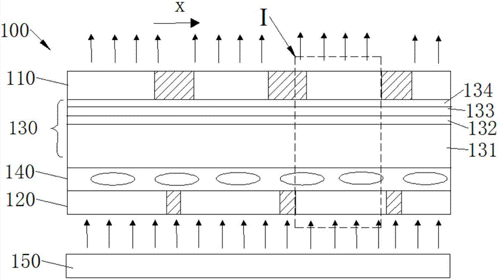
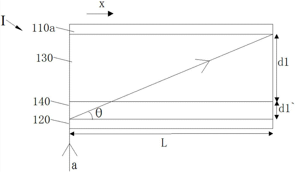
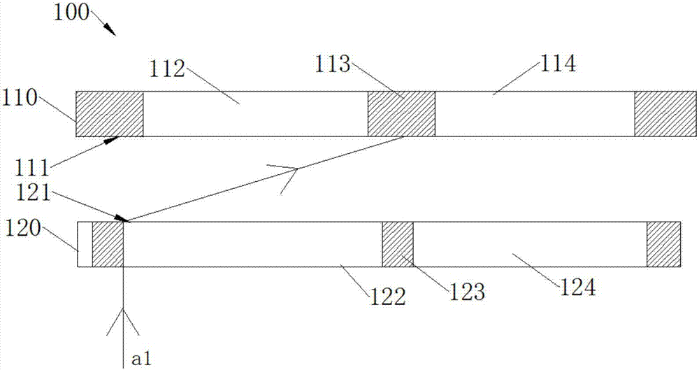
[0036] see Figure 5 , the first substrate 110 is a thin film transistor layer, and the second substrate 120 is a color filter substrate. The backlight source 150 is disposed on a side of the thin film transistor layer 110 away from the color filter substrate 120 . The backlight source 150 emits the first light a1 through the third light transmission area 122 and projects to the first light transmission area 112 . The first light-transmitting region 112 and the second light-transmitting region 114 may be opening regions of the thin film transistor layer 110 , and the first light-shielding region 113 may be a metal wiring region (including a thin film transistor and corresponding metal wiring). The third light-transmitting region 122 and the fourth light-transmitting region 124 may be color-resistive sub-pixel regions, and the second light-shielding region 123 may be a black matrix.

[0037] Generally, the area of ​​the light transmission area of ​​the thin film transistor la...

no. 2 example

[0044] see Figure 7 , the first substrate 110 may also be a color filter substrate, and the second substrate 120 may also be a thin film transistor layer. The display substrate further includes a backlight source 150, and the backlight source 150 is disposed on a side of the thin film transistor layer away from the color filter substrate. The backlight source 150 emits the second light a2 through the first light transmission area 112 and projects to the third light transmission area 122 .

[0045] The first light-transmitting region 112 and the second light-transmitting region 114 may be color-resistive sub-pixel regions, and the first light-shielding region 113 may be a black matrix. The third light-transmitting region 122 and the fourth light-transmitting region 124 may be opening regions of the TFT layer 120, and the second light-shielding region 113 may be a second metal wiring region. Wherein, the projected area of ​​the first light shielding area 113 on the second sub...


PUM

PropertyMeasurementUnit
Angleaaaaaaaaaa

Abstract

The invention discloses a display panel. The display panel includes a liquid crystal layer, a first base board and a second base board. The liquid crystal layer is arranged between the first base board and the second base board. A first photic zone, a first shading zone and a second photic zone are successively connected to the first base board. A third photic zone, a second shading zone and a fourth photic zone are sequentially connected to the second base board. The projection area of the first shading zone on the second base board covers the second shading zone. The first shading zone is used for resisting a first ray projecting to the second photic zone when the first ray projects to the first photic zone. The second shading zone is used for resisting a second ray projecting to the fourth photic zone when the second ray projects to the third photic zone. The invention further provides a display device. By the adoption of the display panel and the display device, the problem of ray crosstalk in a sub-pixel area of a color filter layer is solved.

Description

technical field [0001] The invention relates to the technical field of liquid crystal display, in particular to a display panel and a display device with the display panel. Background technique [0002] In a traditional display panel, upper and lower polarizers are usually arranged on opposite sides of the color filter layer, and cooperate with liquid crystal optics to form a color light-emitting panel. In some new technological developments, it is necessary to place a polarizing structure between the color filter layer and the liquid crystal layer. This is based on the consideration of the following two situations: (1) The color filter layer is generally composed of pigments and other components. The tiny particles of pigments have a certain degree of depolarization effect on the polarization state of polarized light. This mechanism will lead to The contrast ratio of the entire display panel is reduced, therefore, a polarizing structure needs to be placed between the color...

Claims


Application Information

Patent Timeline
IPC IPC(8): G02F1/1335G02F1/1362
CPCG02F1/133512G02F1/133514G02F1/136209
Inventor 陈黎暄
Owner SHENZHEN CHINA STAR OPTOELECTRONICS TECH CO LTD
Why Eureka
Try Eureka