

Wafer
A technology of wafers and chips, applied in the direction of electrical components, circuits, semiconductor devices, etc., can solve problems such as poor circuit performance and high noise, and achieve the effect of improving circuit performance and good thermal isolation effect
- Summary
- Abstract
- Description
- Claims
- Application Information
AI Technical Summary
Problems solved by technology
Method used
Image

Examples
Embodiment 1
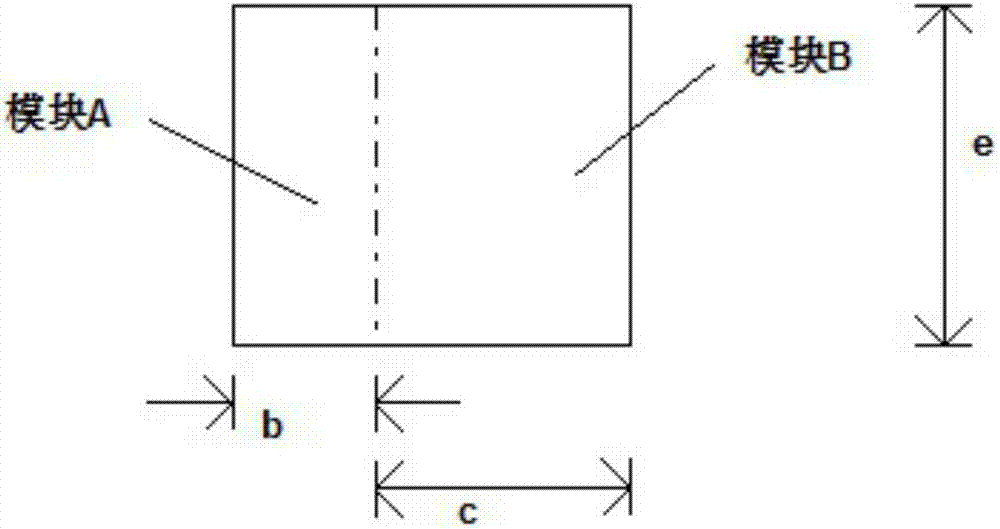
[0031] image 3 shows the schematic structure of the wafer described in the embodiment of the present application Figure 1 , as shown in the figure, the two ends of the connection part of the wafer are respectively connected to one end of the first circuit part and one end of the second circuit part, and the other end of the first circuit part is connected to the second circuit part The other end of the section faces the same direction.
[0032] During specific implementation, the width of the first circuit part and the width of the second circuit part may be the same or different. Assuming that the width of the first circuit part (the left part in the figure) is b, b can be designed as a sensitive analog circuit; the width of the second circuit part (the right part in the figure) is c, and c can be designed as a noise circuit (for example: digital circuit or power circuit), the third part is the connecting part in the middle, which is used for the mutual electrical connect...
Embodiment 2
[0041] Figure 5 shows the schematic structure of the wafer described in the embodiment of the present application Figure II , as shown in the figure, the two ends of the connecting part are respectively connected to the middle part of the first circuit part and the middle part of the second circuit part, and the straight line where the two ends of the first circuit part is located is in line with the second The straight lines where the two ends of the circuit part are located are parallel, and the structure formed by the first circuit part, the connecting part and the second circuit part has two concave parts, and the opening directions of the two concave parts are opposite.
[0042]As shown in the figure, the difference from the first embodiment is that the connecting portion is arranged at the middle position in the up-down direction of the left part and the right part.
[0043] Figure 6 A schematic diagram showing the wafer described in the embodiment of the present ap...
Embodiment 3
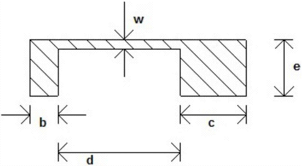
[0049] Figure 7 shows the schematic structure of the wafer described in the embodiment of the present application Figure three , as shown in the figure, the connecting portion includes a first horizontal end, a second horizontal end and a U-shaped portion, the first horizontal end is used to connect the first circuit portion and the U-shaped portion, and the second horizontal end is used for For connecting the U-shaped part and the second circuit part.
[0050] In the embodiment of the present application, the connecting part may be designed in a curved shape, such as a U shape.
[0051] Figure 8 A schematic of the wafer shown in the pro example itself Figure three , as shown in the figure, the plurality of wafers may be arranged sequentially, and the dot-dash line describes the position for dicing after the wafer is manufactured.
[0052] In a specific implementation, there may be multiple U-shaped parts, and the connecting part may further include a third horizontal ...
PUM
 Abstract
Description
Claims
Application Information