[0005]Disclosed herein are complementary current sink and
current source circuits, a charge pump circuit that incorporates the current sink and current source circuits, and a
phase locked loop that incorporates the charge pump circuit. The current source and current sink circuits each have a current mirror circuit that biases a
transistor connected to an output node. The transistor is adapted to adjust the output voltage at the output node (i.e., the transistor is either a current sink transistor or current source transistor, depending upon the type of circuit). The current source and current sink circuits each further have a two-stage feedback
amplifier (i.e., a common-gate feedback amplifier connected in series with a common-source amplifier) to sense the drain voltage of the current mirror circuit and to control the
gate voltage of the transistor in order to stabilize the drain voltage of the current mirror circuit independent of variations in the output voltage at the output node. In both the current sink and current source circuits, the two-stage feedback amplifier increases the output resistance of the current mirror circuit and consequently increases the output resistance at the output node. This configuration allows for a wide operation
voltage range and ensures good
circuit performance under a very low power supply. Due to the increased output resistances at the output node, a charge pump circuit that incorporates the current sink and current source circuits generates highly matched charging and discharging currents. Furthermore, due to the highly matched charging and discharging currents in the charge pump circuit, a PLL circuit that incorporates the charge pump circuit exhibits minimal shifts in PLL
loop bandwidth and minimal degradation of PLL locking speed and
jitter performance across its full frequency range.
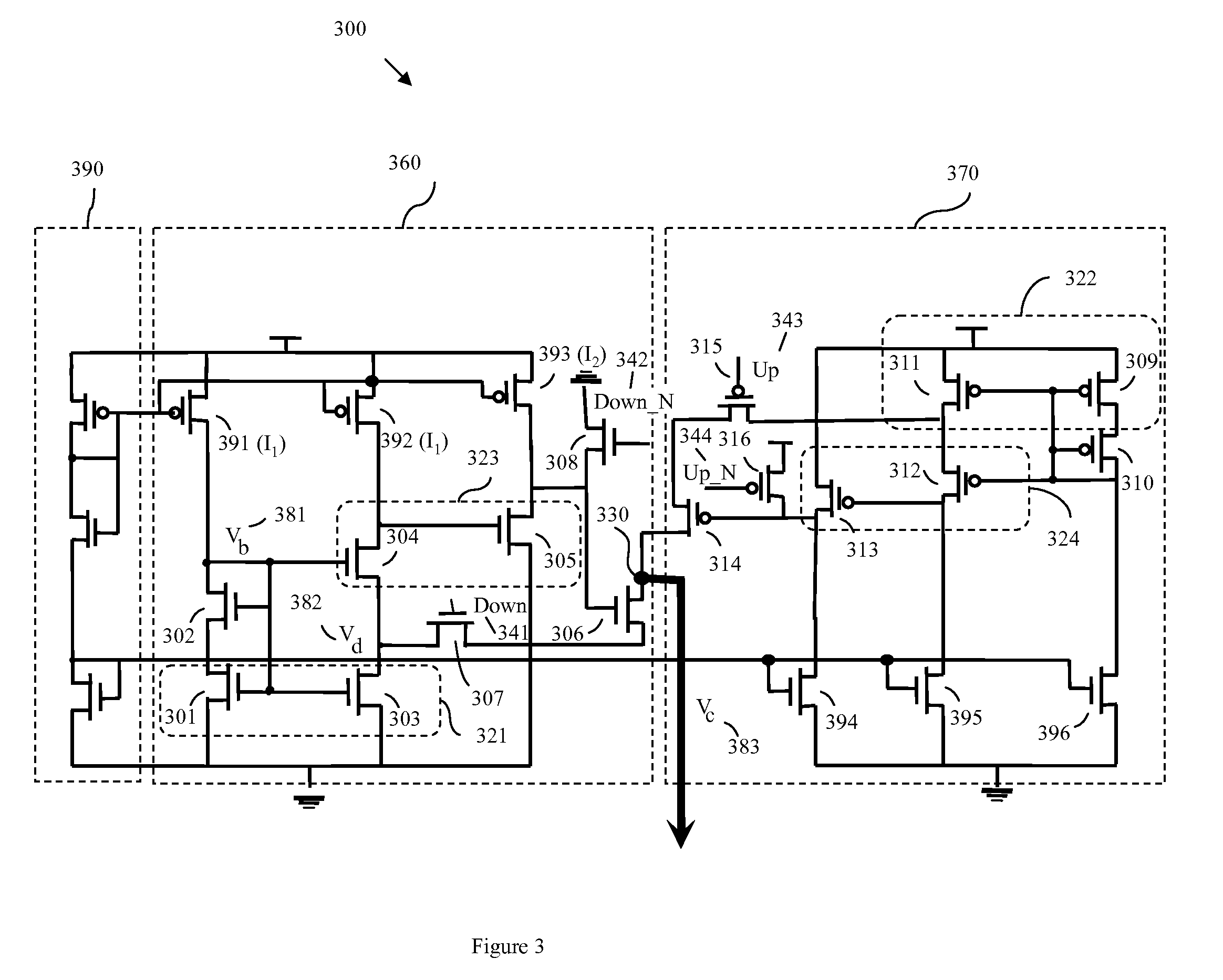
[0006]More particularly, disclosed herein is an embodiment of a current sink circuit that comprises a current sink device (e.g., N-type
field effect transistor (N-FET)) adapted to decrease an output voltage at an output node in response to a received
signal. The current sink circuit can further comprise a current mirror circuit connected to the source of the current sink device and adapted to supply a bias current (i.e., a
reference current from a biasing circuit) to the current sink device. A digital switch can be connected between the current sink device and the current mirror circuit. This digital switch (e.g., an N-FET or other suitable digital switch) can be adapted to turn on in response to a
signal (e.g., a “Down” signal) in order to establish a current path from the current mirror circuit through the current sink device to the output node, thereby decreasing the output voltage at the output node. An additional digital switch (e.g., an N-FET or other suitable digital switch) can be connected to the gate of the current sink device. This additional digital switch can be adapted to turn on in response to an opposite signal (e.g., a “Down_N” signal) in order to pull down the
gate voltage of the current sink device and, thereby, to break the current path. Additionally, a two-stage feedback amplifier can be connected to both the current mirror circuit and the current sink device. This two-stage feedback amplifier (e.g., a common-gate feedback amplifier connected in series with a common-source amplifier) can be adapted to sense a drain voltage of the current mirror circuit and to control a gate voltage of the current sink device in order to stabilize the drain voltage of the current mirror circuit independent of variations (e.g., decreases) in the output voltage at the output node. This two-stage feedback amplifier further adds to (i.e., increases) the output resistance of the current mirror circuit and, thereby, increases the output resistance of the current sink circuit at the output node as compared to a single-stage feedback amplifier.
[0007]Similarly, disclosed is an embodiment of a complementary current source circuit that comprises a current source device (e.g., a P-type
field effect transistor (P-FET)) adapted to increase an output voltage at the output node in response to a received signal. The current source circuit can further comprise a current mirror circuit connected to the source of the current source device and adapted to supply a bias current (i.e., a
reference current from a biasing circuit) to the current source device. A digital switch (e.g., a P-FET or other suitable digital switch) can be connected between the current source device and the current mirror circuit. This digital switch can be adapted to turn on in response to a signal (e.g., an “Up” signal) in order to establish a current path from the current mirror circuit through the current source device to the output node, thereby increasing the output voltage at the output node. An additional digital (e.g., a P-FET or other suitable digital switch) switch can be connected to a gate of the current source device. This additional digital switch can be adapted to turn on in response to an opposite signal (e.g., an “Up_N” signal) in order to pull down the gate voltage of the current source device and, thereby, to break the current path. Additionally, a two-stage feedback amplifier can be connected to both the current mirror circuit and the current source device. This two-stage feedback amplifier (e.g., a common-gate feedback amplifier connected in series with a common-source amplifier) can be adapted to sense a drain voltage of the current mirror circuit and to control a gate voltage of the current source device in order to stabilize the drain voltage of the current mirror circuit independent of variations (e.g., increases) in the output voltage at the output node. This two-stage feedback amplifier further increases the output resistance of the current mirror circuit and, thereby, increases the output resistance of the current source circuit at the output node as compared to a single-stage feedback amplifier.
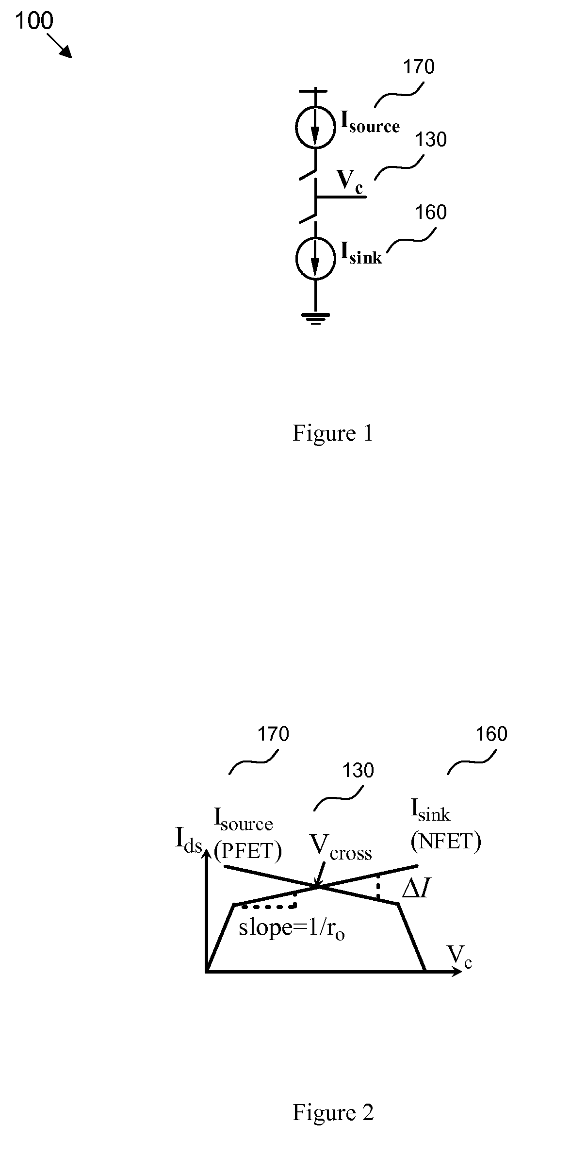
[0011]Consequently, the first transistor and the third transistor in combination comprise the current mirror circuit. Additionally, the fourth transistor and the fifth transistor in combination comprise the two-stage feedback amplifier (i.e., a
common gate amplifier connected in series with a
common source amplifier), which can sense the drain voltage of the current mirror circuit (i.e., can sense the drain voltage at the drain of the third transistor) and can control the gate voltage of the current sink device (i.e., can control the gate voltage of the sixth transistor) so as to a stabilize the drain voltage of the current mirror circuit independent of variations in the output voltage at the output node. An overall feedback
amplifier gain of the two-stage feedback amplifier will be approximately equal to the product of each
gain from each stage of the two-stage feedback amplifier (i.e., equal to the
common gate amplifier gain multiplied by the
common source amplifier gain). By increasing the overall amplifier
gain, the two-stage feedback amplifier significantly increases the current mirror circuit output resistance and, thereby, the output resistance at the output node. Additionally, the use of the
common gate amplifier in the first stage of the two-stage feedback amplifier reduces the voltage requirement to the drain of the third transistor (i.e., to the output of the current mirror circuit) and thereby, increases the operation
voltage range of the circuit. Finally, if the
aspect ratio of the first transistor is half that of the other transistors, when the circuit conducts the current in the third transistor will be twice that in the first transistor (i.e., twice the
reference current from the biasing circuit), whereas the current in the sixth transistor will be the same as that in the first transistor (i.e., the same as the reference current from the biasing circuit).
[0012]The current sink circuit and current source circuit embodiments can further comprise a
capacitor (e.g., a Miller
capacitor) connected between the gate and the drain of the second stage of the two-stage feedback amplifier. That is, the
capacitor can be connected between the gate and drain of the fifth transistor (i.e.,
common source amplifier). This additional capacitor increases the
feedback capacitance and, thereby, increases the circuit
phase margin in order to improve circuit stability.
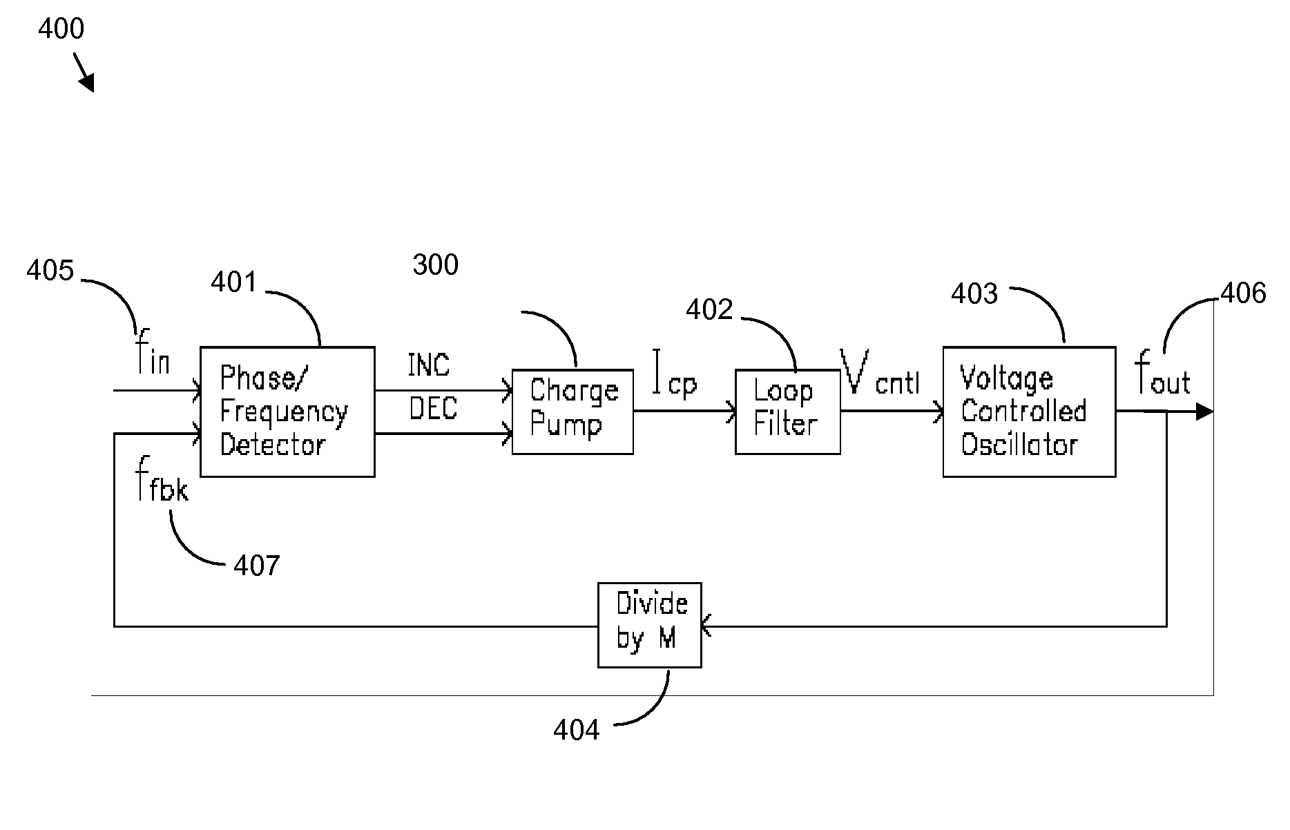
[0015]Also disclosed is an embodiment of a
phase locked loop (PLL) circuit that incorporates the charge pump circuit embodiment, described above. Specifically, a PLL circuit is disclosed that comprises a
phase frequency detector, a charge pump, and a
voltage control oscillator (VCO). As with conventional PLL circuits, this
phase frequency detector can be adapted to detect a
phase difference between a reference frequency and a feedback frequency that is output to the
phase frequency detector from the VCO (e.g., via an optional divide-by-M device). The phase frequency
detector can be adapted to generate a correction signal (i.e., either an increase signal or a decrease signal), depending upon the
phase difference detected. The charge pump circuit can be connected to the phase frequency
detector (e.g., via a
loop filter). The charge pump circuit embodiment can be adapted to receive increase signals (e.g., “Up”, “Down_N”) and decrease signals (e.g., “Down”, “Up_N”) from the phase frequency detector. Additionally, as discussed above, the charge pump circuit can be adapted to adjust an output voltage to the VCO depending upon whether an increase signal or a decrease signal is received (see detailed discussion above regarding functions of current sink circuit and current source circuit). The VCO can be adapted to receive the adjusted voltage at the output node of the charge pump (e.g., via a
loop filter) and further to adjust the output frequency based on that output voltage. Due to the highly matched charging and discharging currents in the charge pump, this PLL circuit exhibits minimal shifts in PLL
loop bandwidth and minimal degradation of PLL locking speed and jitter performance across its full frequency range.

