Memory and method for forming same, semiconductor device
A memory and conductor technology, applied in semiconductor devices, semiconductor/solid-state device manufacturing, electric solid-state devices, etc., can solve problems affecting memory performance, component size reduction, and large contact resistance
- Summary
- Abstract
- Description
- Claims
- Application Information
AI Technical Summary
Problems solved by technology
Method used
Image
Examples
Embodiment 1
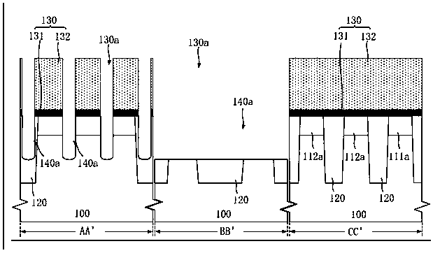
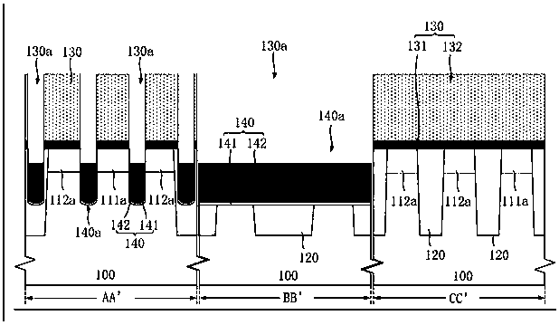
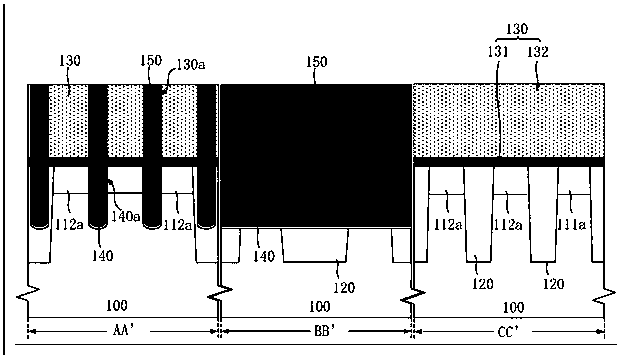
[0150] figure 1 It is a schematic flow chart of the forming method of the memory in Embodiment 1 of the present invention, such as figure 1 As shown, in the forming method of the memory shown in this embodiment, the contact window defined by the first isolation barrier and the second isolation barrier is directly used, and under the limitation of the first isolation barrier and the second isolation barrier, the A conductive layer is aligned and filled in the contact hole to form a storage node contact. Compared with the traditional method, in this embodiment, when defining the contact window corresponding to the storage node contact, it is not necessary to use an additional photolithography process. The following is attached figure 1 The method of forming the memory in this embodiment will be described in detail.
[0151] Figure 2a is a top view of the memory forming method in Embodiment 1 of the present invention when step S110 is executed, Figure 2b for Figure 2a Th...
Embodiment 2
[0206] The difference from Embodiment 1 is that in the memory forming method of this embodiment, the surface of the first isolation barrier corresponding to the word line conductor is higher than the surface of the second isolation barrier corresponding to the bit line, so that the first isolation barrier can be used to automatically A continuous conductive layer is formed in an aligned manner, and the conductive layer extends along the first direction, thereby facilitating adjustment of the extending direction of the storage node contact when the storage node contact is prepared. Compared with the traditional forming method, in this embodiment, there is no need to additionally form a redistribution layer to adjust the extension direction of the storage node contact by photolithography process, which is beneficial to simplify the process.
[0207] Figure 9 It is a schematic flow chart of the forming method of the memory in Embodiment 2 of the present invention, such as Figu...
Embodiment 3
[0231] The present invention also provides a memory in which a contact window corresponding to a storage node contact is directly defined by a first isolation barrier corresponding to a word line conductor and a second isolation barrier corresponding to a bit line, so that the defined The boundaries of the contact windows respectively extend to positions close to the bit line and close to the sidewalls of the word line conductors. Therefore, the projection of the contact window in the height direction can not only cover the second contact region, but also the projected area of the contact window is larger than that of the second contact area. The projected area of the second contact area in the height direction. In this way, on the one hand, the formed storage node contact can be completely electrically connected to the second contact region; on the other hand, there is a larger contact area between the storage node contact and the second contact region, which is beneficial...
PUM
 Abstract
Description
Claims
Application Information


