Mask, hole forming method, display substrate forming method, display substrate and display device

A technology for display substrates and masks, which is applied in the photoengraving process of the pattern surface, the originals for opto-mechanical processing, optics, etc., and can solve the problems of the decrease of the pixel aperture ratio, the influence of the connectivity, and the large difference in the pitch of the via holes. , to achieve the effect of reducing contact resistance, improving connectivity, and reducing level difference

Inactive Publication Date: 2017-10-13
BOE TECH GRP CO LTD +1
View PDF4 Cites 13 Cited by
  • Summary
  • Abstract
  • Description
  • Claims
  • Application Information

AI Technical Summary

Problems solved by technology

[0003] At present, the shape of the via hole is usually designed as a rectangle (that is, the cross section parallel to the plane of the display substrate is square or rectangular). Area, that is, the area at the bottom of the via hole) is small, which makes the contact resistance of the via hole large, resulting in poor connectivity between the upper and lower conductive layers
Increasing the size of the via hole can effectively reduce the contact resistance of the via hole and enhance the connectivity, but the large size of the via hole will lead to a decrease in the aperture ratio of the pixel (Pixel), and may also cause Mura related to the diffusion of the alignment film (PI).
[0004] At the same time, as the resolution requirements of display products become higher and higher, and the charging time is reduced, it is often necessary to use a thicker insulating layer (PVX (passivation layer) or ORG (organic film), etc.) to reduce the storage capacitance (Cst) to improve charging rate, when the thickness of the insulating layer used to set the via hole is large, the existing rectangular via hole design will result in a large slope angle on the four walls of the via hole, so that the step difference of the via hole is large, and the upper conductive layer is entering It is easy to break when it is in the hole, which affects the connectivity

Method used


Image

  • Mask, hole forming method, display substrate forming method, display substrate and display device
  • Mask, hole forming method, display substrate forming method, display substrate and display device
  • Mask, hole forming method, display substrate forming method, display substrate and display device

Examples


Embodiment Construction

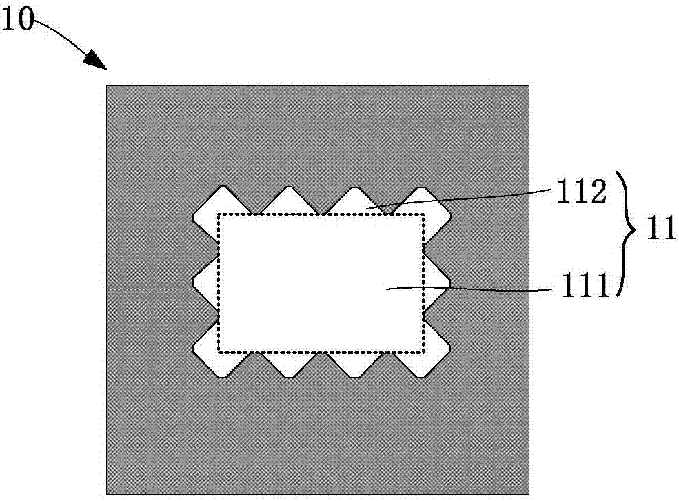
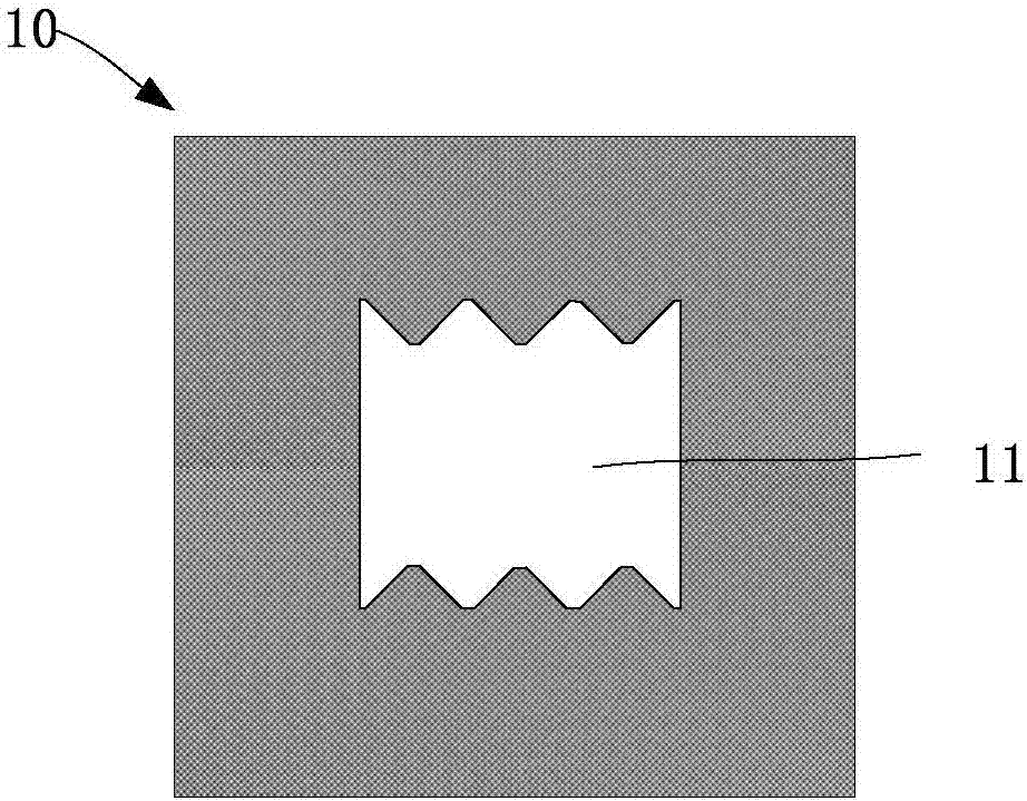
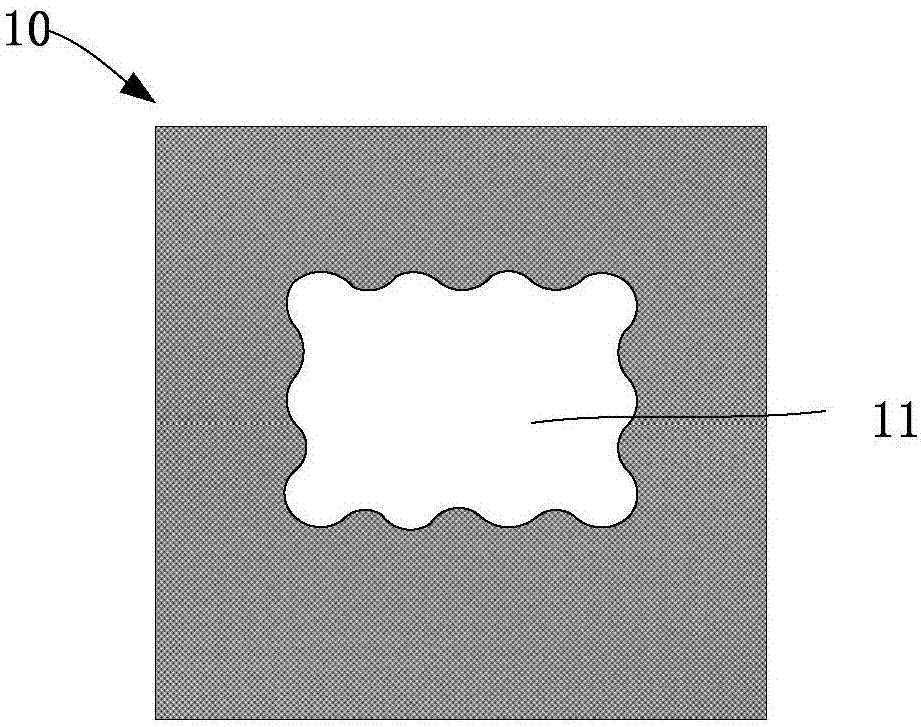
[0039] In order to solve the problem that the contact area of ​​the via hole between the upper and lower conductive layers electrically connected through the via hole is small on the existing display substrate, resulting in a large contact resistance of the via hole, and the large difference of the via hole section affects the connectivity. The present invention provides a A method for forming a mask plate, a via hole and a display substrate, a display substrate and a device, which can increase the contact area of ​​the via hole between the upper and lower conductive layers electrically connected through the via hole, reduce the contact resistance of the via hole and the level difference of the via hole, Improve connectivity.

[0040] In order to make the purpose, technical solutions and advantages of the embodiments of the present invention more clear, the following will clearly and completely describe the technical solutions of the embodiments of the present invention in conj...


PUM


Abstract

The invention provides a mask, a hole forming method, a display substrate forming method, a display substrate and a display device. The mask is used for forming a hole on a film, and comprises a light-transmittable pattern used for forming the hole; and the light-transmittable pattern has a curved edge. Because the light-transmittable pattern on the mask has the curved edge, the bottom of the hole formed by adoption of the mask also has the curved edge; therefore, the length of a contact boundary line of upper and lower conductive layers electrically connected through the hole can be increased; the contact resistance between the upper and lower conductive layers can be reduced; the connectivity between the upper and lower conductive layers can be improved; in addition, in an exposure process for forming the hole, the transmission amount of light at the edge of the light-transmittable pattern is relatively low; only a part of thickness of the film corresponding to the part can be exposed; therefore, the slope angle of the inner wall of the formed hole is relatively small; the segment gap of the hole can be reduced; breakage of the upper conductive layer in the hole can be avoided; and thus, the connectivity is further improved.

Description

technical field [0001] The invention relates to the field of display technology, in particular to a method for forming a mask, a via hole and a display substrate, a display substrate and a device. Background technique [0002] In the design of the display substrate, in order to realize the electrical connection, different conductive layers (such as metal layers or ITO layers, etc.) need to be connected through holes (Hole), and the size and shape design of the hole determines the connectivity between different conductive layers. and contact resistance. [0003] At present, the shape of the via hole is usually designed as a rectangle (that is, the cross section parallel to the plane of the display substrate is square or rectangular). The area, that is, the area at the bottom of the via hole) is small, so that the contact resistance of the via hole is relatively large, resulting in poor connectivity between the upper and lower conductive layers. Increasing the size of the vi...

Claims


Application Information

Patent Timeline
Patent Type & Authority Applications(China)
IPC IPC(8): G03F1/54G02F1/1362H01L27/12
CPCH01L27/1244H01L27/1288G02F1/136227G03F1/54G03F1/36G03F1/38H01L27/1222
Inventor 王小元杨妮方琰齐智坚李云泽许亨艺
Owner BOE TECH GRP CO LTD
Why Eureka
Try Eureka