


Quick Research
Generate reliable direction feasibility study reports for your R&D in just a few steps.

Technical Q&A
Discover and master advanced knowledge NOW. Basics, ideas, possibilities, all at once.

Find Solutions
As an expert in R&D theories, this can generate solutions to your technical problems instantly.

Evaluate Feasibility
Analyze your overall solution with one click, know your potential R&D risks in advance.

Monitor Landscape
Get weekly tech updates, stay abreast of the latest tech innovations and key insights.
COB encapsulation structure protected by Zener diode
A Zener diode and packaging structure technology, applied in electrical components, electrical solid devices, circuits, etc., can solve the problems of COB packaging structure protection, LED chip lighting and heat dissipation effects, and achieve the effect of multiple installation spaces
- Summary
- Abstract
- Description
- Claims
- Application Information
AI Technical Summary
Problems solved by technology
Method used
Image

Examples
Embodiment 1
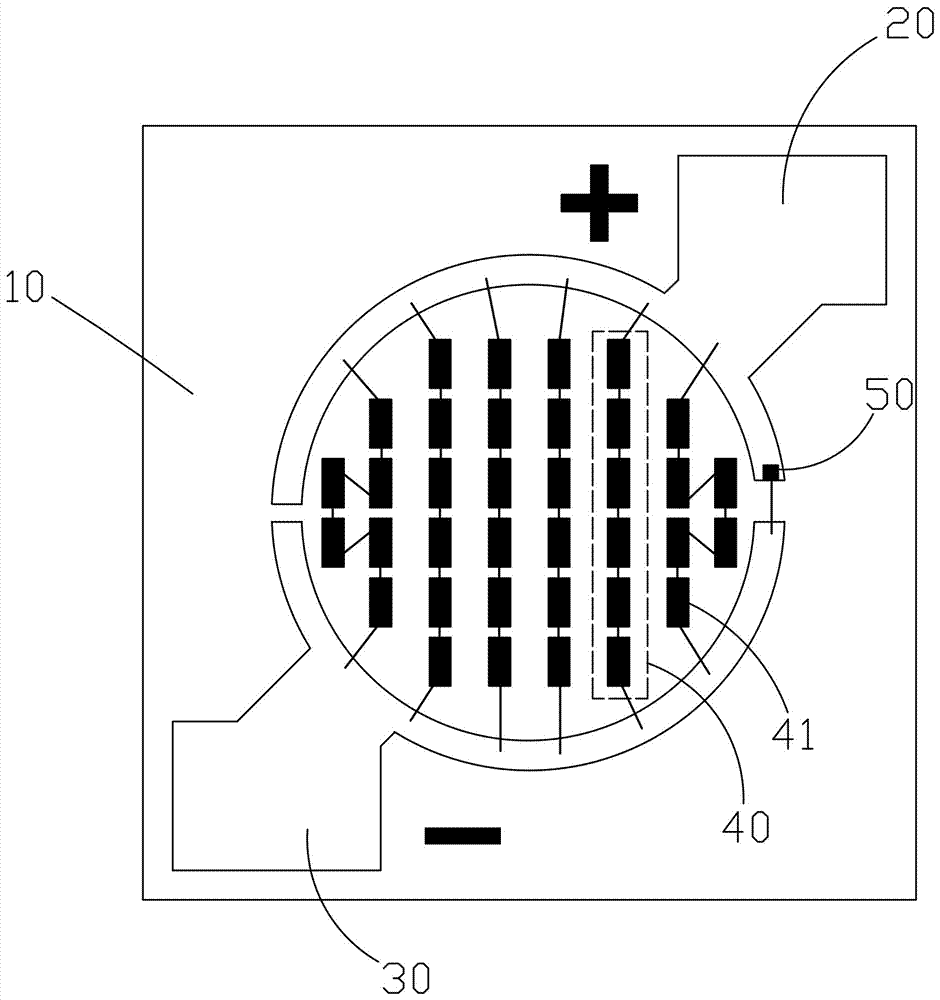
[0029] See figure 1 with 2 As shown, the present invention relates to a COB packaging structure with zener diode protection, the implementation of the first embodiment includes a substrate 10, a positive electrode 20, a negative electrode 30 and an LED chip group 40, a positive electrode 20, and a negative electrode 30 And the LED chipset 40 is all arranged on the substrate 10, wherein the substrate 10 is a substrate with a certain heat dissipation function, and its shape includes but not limited to any one of rectangle, circle, and ellipse; the LED chipset 40 can be one or more, each LED chip group 40 is composed of multiple LED chips in series, and the two ends of the LED chip group 40 are electrically connected to the positive electrode 20 and the negative electrode 30 respectively, thereby forming a COB device of the LED. Specifically, the LED chip 41 is bonded on the substrate 10 by a crystal-bonding glue, and the fluorescent glue covers the upper surface of each LED chi...
Embodiment 2
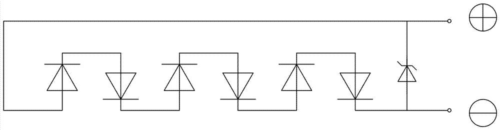
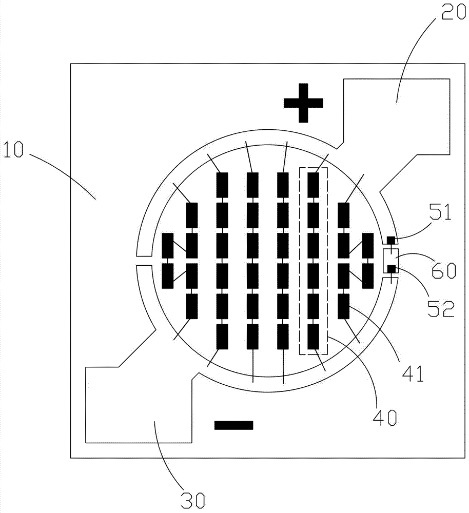
[0032] In the second embodiment, two (or multiple) zener diodes in the same direction or in the opposite direction are connected in series to perform bidirectional protection for the COB device. For details, please refer to image 3 with 4 As shown, the present invention relates to a COB packaging structure with zener diode protection, and the implementation of the second embodiment includes a substrate 10, a positive electrode 20, a negative electrode 30 and an LED chip group 40, a positive electrode 20, a negative electrode 30 and the LED chipset 40 are both disposed on the substrate 10 . In order to suppress transient voltages (caused by electrostatic discharge or high-voltage transient signals), in the second embodiment, the COB package structure further includes two Zener diodes and a copper foil layer 60, which are the first Zener diode 51 and the second copper foil layer 60 respectively. Two zener diodes 52, wherein the first zener diode 51 and the second zener diode ...
Embodiment 3
[0043] In the third embodiment, two zener diodes in the same direction or in the opposite direction are connected in series to protect the COB device bidirectionally. For details, please refer to Figure 5 with 6 As shown, the present invention relates to a COB packaging structure with zener diode protection, and the implementation of the third embodiment includes a substrate 10, a positive electrode 20, a negative electrode 30 and an LED chip group 40, a positive electrode 20, a negative electrode 30 and the LED chipset 40 are both disposed on the substrate 10 . In order to suppress transient voltages (caused by electrostatic discharge or high-voltage transient signals), in the third embodiment, the COB package structure further includes two Zener diodes and a copper foil layer 60, which are the first Zener diode 51 and the second copper foil layer 60 respectively. Two zener diodes 52, wherein the first zener diode 51 and the second zener diode 52 are installed on the posit...
PUM
 Abstract
Description
Claims
Application Information
 - R&D Engineer
- R&D Manager
- IP Professional
- Industry Leading Data Capabilities
- Powerful AI technology
- Patent DNA Extraction
Browse by: Latest US Patents, China's latest patents, Technical Efficacy Thesaurus, Application Domain, Technology Topic, Popular Technical Reports.
© 2024 PatSnap. All rights reserved.Legal|Privacy policy|Modern Slavery Act Transparency Statement|Sitemap|About US| Contact US: help@patsnap.com