Self alignment contact scheme, semiconductor device and method for manufacturing the same

A semiconductor, conductive contact technology, applied in the direction of semiconductor devices, semiconductor/solid-state device manufacturing, electrical components, etc., can solve problems such as short circuit of conductive parts

Active Publication Date: 2017-10-20
TAIWAN SEMICON MFG CO LTD
View PDF5 Cites 25 Cited by
  • Summary
  • Abstract
  • Description
  • Claims
  • Application Information

AI Technical Summary

Problems solved by technology

[0004] In particular, as designs shrink, conductive features connected to layers above and below may short out if the conductive features are misaligned

Method used


Image

  • Self alignment contact scheme, semiconductor device and method for manufacturing the same
  • Self alignment contact scheme, semiconductor device and method for manufacturing the same
  • Self alignment contact scheme, semiconductor device and method for manufacturing the same

Examples


Embodiment

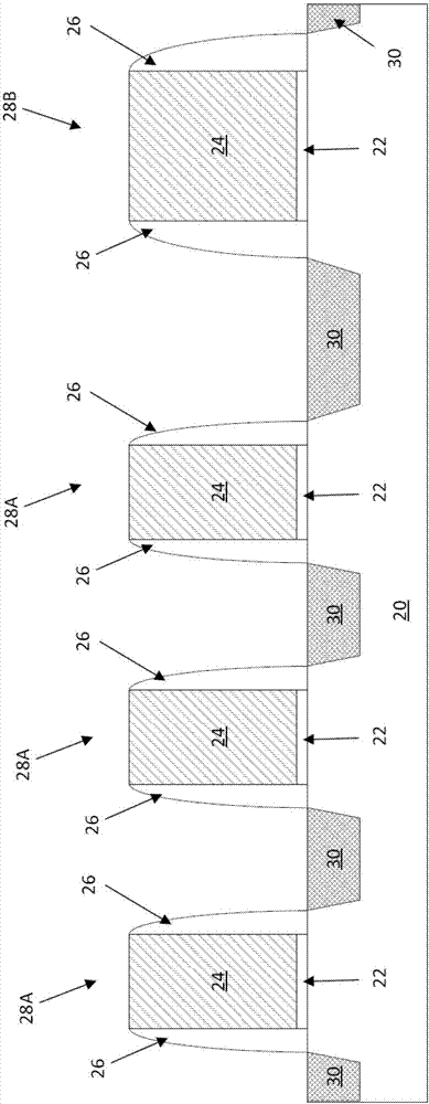
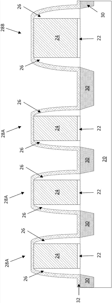
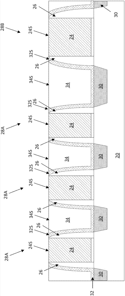
[0059] An embodiment is a method including: forming a first gate over a substrate, the first gate having first gate spacers on opposite sidewalls of the first gate; and forming a first gate over the first gate A hard mask layer; a second hard mask layer is formed above the first hard mask layer, the second hard mask layer has a different material composition from the first hard mask layer; adjacent to the first gate and in the A first dielectric layer is formed above a gate; a first opening through the first dielectric layer is etched to expose a portion of the substrate, and at least a portion of the second hard mask layer is exposed in the first opening; and a conductive material is used to fill A first opening; and removing the second hard mask layer and removing the conductive material and the portion of the first dielectric layer located above the first hard mask layer to form a first conductive contact in the remaining first dielectric layer.

[0060] In an embodiment, the ...


PUM


Abstract

An embodiment is a method including forming a first gate over a substrate, the first gate having first gate spacers on opposing sidewalls, forming a first hard mask layer over the first gate, forming a second hard mask layer over the first hard mask layer, the second hard mask layer having a different material composition than the first hard mask layer, forming a first dielectric layer adjacent and over the first gate, etching a first opening through the first dielectric layer to expose a portion of the substrate, at least a portion of the second hard mask layer being exposed in the first opening, filling the first opening with a conductive material, and removing the second hard mask layer and the portions of the conductive material and first dielectric layer above the first hard mask layer to form a first conductive contact in the remaining first dielectric layer. The invention also provides a self alignment contact scheme, a semiconductor device and a method for manufacturing the same.

Description

Technical field [0001] The embodiments of the present invention generally relate to the field of semiconductor technology, and more specifically, to semiconductor structures and methods of forming the same. Background technique [0002] Semiconductor devices are used in various electronic applications, for example, such as personal computers, cell phones, digital cameras, and other electronic devices. Semiconductor devices are usually manufactured by the following steps: successively depositing an insulating or dielectric layer, a conductive layer, and a layer of semiconductor material over a semiconductor substrate; and using photolithography to pattern the multiple material layers to form circuit components and layers thereon element. [0003] The semiconductor industry continues to improve the integration density of individual electronic components (eg, transistors, diodes, resistors, capacitors, etc.) by continuously reducing the minimum component size, thereby allowing more c...

Claims


Application Information

Patent Timeline
Patent Type & Authority Applications(China)
IPC IPC(8): H01L21/768H01L21/336H01L29/78
CPCH01L21/76802H01L21/76897H01L29/66477H01L29/785H01L21/76834H01L29/6656H01L29/66545H01L21/823475H01L29/41783H01L29/665H01L29/78
Inventor 何彩蓉许光源郑培仁
Owner TAIWAN SEMICON MFG CO LTD
Why Eureka
Try Eureka