Wire bonding apparatus and bonding method of implantable micro-electronic product

A technology of wire bonding and microelectronics, which is applied in the field of biomedical engineering, can solve the problems of complicated wire bonding process and high cost, and achieve the effect of safe and stable bonding strength, low cost, and guaranteed safety and reliability

Pending Publication Date: 2017-10-27
HANGZHOU NANOCHAP ELECTRONICS CO LTD +1
View PDF0 Cites 0 Cited by
  • Summary
  • Abstract
  • Description
  • Claims
  • Application Information

AI Technical Summary

Problems solved by technology

The wire bonding process is relatively complicated and the cost is high, which is also the reason for limiting the promotion and use of micro-devices in the field of bioengineering

Method used


Image

  • Wire bonding apparatus and bonding method of implantable micro-electronic product
  • Wire bonding apparatus and bonding method of implantable micro-electronic product
  • Wire bonding apparatus and bonding method of implantable micro-electronic product

Examples


Embodiment 1

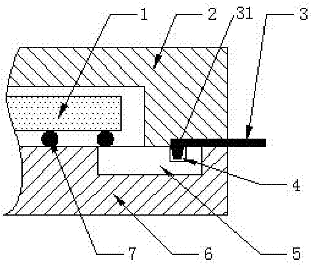
[0032] Such as figure 1 The shown wire bonding device for implantable microelectronic products of the present invention includes a plurality of wire connectors 5 embedded in the package base, and one end of the wire connectors 5 is connected to the package base and the housing 2 The chip 1 between them is electrically connected, the number of the wire connector 5 is set according to the connection point of the chip 1, and the position is set correspondingly according to the position of the connection point of the chip 1, and the other end is provided with a card slot 4, preferably Such as figure 1 and figure 2 As shown, the card slot 4 is formed by digging a groove on the wire connector 5, the card slot 4 is used to fix the end 31 of the cable 3, and the middle section of the cable 3 is pressed fit between the package base and the case 2.

[0033] In a preferred embodiment, the slot 4 of the wire connector 5 and the end 31 of the cable 3 are fused and welded with a small a...

Embodiment 2

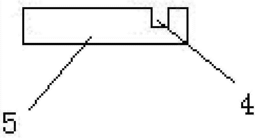
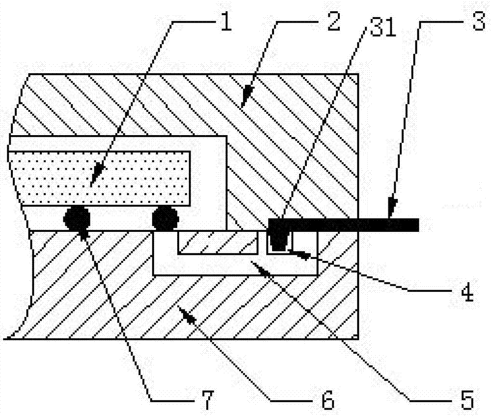
[0040] In this example, if image 3 The shown wire bonding device for implantable microelectronic products of the present invention includes a plurality of wire connectors 5 embedded in the package base, and one end of the wire connectors 5 is connected to the package base and the housing 2 The chip 1 is connected between them, the number of the wire connectors 5 is set according to the connection point of the chip 1, and the position is set correspondingly according to the position of the connection point of the chip 1, and the other end is provided with a card slot 4, preferably as image 3 and Figure 4 shown. A welding slot 51 is also formed inside the clamping slot 4 , wherein the clamping slot 4 is used to fix the end 31 of the cable 3 . The fixing groove 51 is filled with the same material as that of the packaging shell 2, this embodiment can solve the defect of incompatibility of the packaging interface, and provides a guarantee of airtight packaging.

Embodiment 3

[0042] In this embodiment, a wire bonding device method for implantable microelectronic products is provided, including the following steps:

[0043] S1: Pre-embed a plurality of wire connectors 5 in the package base. In practice, the base material of the package base and the wire connectors are formed by melting or sintering. The mechanical properties are good, and the chip 1 is passed through Flip-chip welding is electrically connected to one end of the wire connector 5;

[0044] S2: After physically inserting the end 31 of the cable 3 into the card slot 4, a small amount of solder fusion welding is performed on the contact between the two; and the method of micro solder fusion welding is a well-known technical means in the welding field, and is adopted in the present invention. A small amount of solder fusion welding has a low melting point and small diffusion, and it needs to maintain a long-term effective connection.

[0045] S3: Finally, the casing 2 is hermetically bon...


PUM


Abstract

The invention relates to a wire bonding apparatus and bonding method of an implantable micro-electronic product. The wire bonding apparatus comprises multiple wire connecting pieces embedded in a packaging substrate; one ends of the wire connecting pieces are connected with chips arranged between the packaging substrate and a shell while clamping grooves used for fixing ends of flat cables are formed in the other ends; and a convex structure is arranged on the end of each flat cable, and the middle section of each flat cable is laminated between the packaging substrate and the shell. Single point processing is avoided in the processing process; accurate alignment is realized in the connecting process through the clamping grooves and the ends; physical embedding in fixed positions is preformed, so that high connecting rate is achieved; a small bonding area is needed in welding, so that safe and stable bonding strength is achieved; by virtue of the design of the clamping grooves, diffusion of solder on the substrate interface can be avoided, so that unnecessary short circuit can be prevented and circuit connection reliability is realized; in addition, the parts are high in biocompatibility, and by depositing the biocompatible coating layer for multiple times, safety and reliability after implantation can be ensured; and the flat cables and corresponding wire connecting pieces can be connected rapidly, so that relatively low cost is achieved.

Description

technical field [0001] The invention relates to a wire bonding device and a bonding method for implantable microelectronic products, belonging to the technical field of biomedical engineering. Background technique [0002] Microelectronics products have become an indispensable and important part of our lives. With the development of science and technology, microelectronics products play an important role in the medical field. It is an effective tool for establishing connections between humans or animals and external devices. It can More direct and accurate treatment monitoring for specific diseases. Implantable electronic products need to be packaged to connect with each other to provide signal transmission. Long-term safe and effective connection methods have become the research goals of various scientific and technological workers. Many breakthroughs have been made in related research in this field around the world. [0003] At present, in the field of biomedicine, there ...

Claims


Application Information

Patent Timeline
Patent Type & Authority Applications(China)
IPC IPC(8): H01L21/60
CPCH01L2224/16225H01L24/741H01L24/745H01L24/91
Inventor 王健陈景雄杨旭燕杨佳威
Owner HANGZHOU NANOCHAP ELECTRONICS CO LTD
Why Eureka
Try Eureka