Organic light-emitting diode display panel and production method thereof

A technology for light-emitting diodes and display panels, which is used in the manufacture of semiconductor/solid-state devices, electrical components, and electrical solid-state devices, and can solve problems such as poor display of OLED display panels.

Active Publication Date: 2017-10-27
BOE TECH GRP CO LTD
View PDF3 Cites 14 Cited by
  • Summary
  • Abstract
  • Description
  • Claims
  • Application Information

AI Technical Summary

Problems solved by technology

[0004] In order to solve the above technical problems, the present invention provides an organic light emitting diode display panel and its manufacturing m

Method used


Image

  • Organic light-emitting diode display panel and production method thereof
  • Organic light-emitting diode display panel and production method thereof
  • Organic light-emitting diode display panel and production method thereof

Examples


Embodiment 1

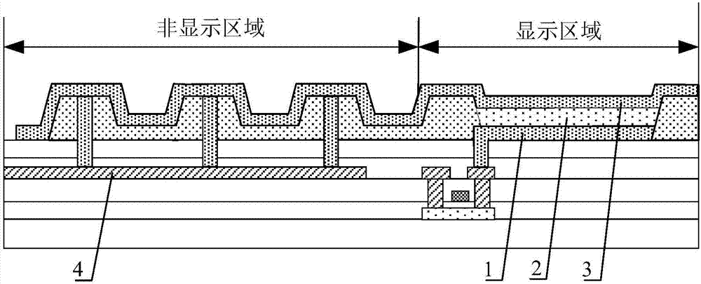
[0061] figure 2 A schematic structural diagram of an OLED display panel provided in Embodiment 1 of the present invention, as shown in figure 2 As shown, the OLED display panel provided by the embodiment of the present invention includes: a first substrate and a second substrate oppositely arranged; the first substrate includes a first lead 11 connected to a cathode 12; the second substrate includes a second lead 11 connected to a peripheral circuit. Lead wire 21 ; the first lead wire 11 is connected to the second lead wire 21 through the connecting portion.

[0062] In this embodiment, the first substrate is an array substrate, and the second substrate is a color filter substrate. It should be understood that the first substrate includes a base 10, and the base 10 includes a display area and a non-display area around the display area. The first substrate It also includes: a thin film transistor 15 arranged on the substrate 10 in the display area, a passivation layer 16 and a...

Embodiment 2

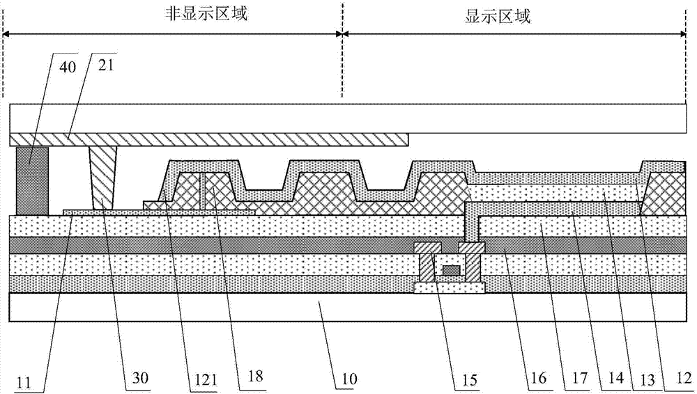
[0076] Based on the above inventive concept, image 3 A schematic structural diagram of an OLED display panel provided in Embodiment 2 of the present invention, as shown in image 3 As shown, the OLED display panel provided by the embodiment of the present invention includes: a first substrate and a second substrate oppositely arranged; the first substrate includes a first lead 11 connected to a cathode 12; the second substrate includes a second lead 11 connected to a peripheral circuit. Lead wire 21 ; the first lead wire 11 is connected to the second lead wire 21 through the connecting portion.

[0077] In this embodiment, the first substrate is an array substrate, and the second substrate is a color filter substrate. It should be understood that the first substrate includes a base 10, and the base 10 includes a display area and a non-display area around the display area. The first substrate It also includes: a thin film transistor 15 arranged on the substrate 10 in the disp...

Embodiment 3

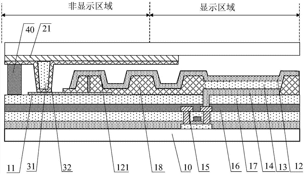
[0092] Based on the above inventive concept, Figure 4 A schematic structural diagram of the OLED display panel provided in Embodiment 3 of the present invention, as shown in Figure 4 As shown, the OLED display panel provided by the embodiment of the present invention includes: a first substrate and a second substrate oppositely arranged; the first substrate includes a first lead 11 connected to a cathode 12; the second substrate includes a second lead 11 connected to a peripheral circuit. Lead wire 21 ; the first lead wire 11 is connected to the second lead wire 21 through the connecting portion.

[0093] In this embodiment, the first substrate is an array substrate, and the second substrate is a color filter substrate. It should be understood that the first substrate includes a base 10, and the base 10 includes a display area and a non-display area around the display area. The first substrate It also includes: a thin film transistor 15 arranged on the substrate 10 in the d...


PUM


Abstract

The embodiment of the invention discloses an organic light-emitting diode display panel and a production method thereof. The organic light-emitting diode display panel comprises a first substrate and a second substrate which are oppositely arranged, wherein the first substrate comprises a first lead wire connected with a negative electrode; the second substrate comprises a second lead wire connected with a peripheral circuit; the first lead wire is connected with the second lead wire through a connecting part. According to the technical scheme adopted by the invention, the negative electrode is connected with the peripheral circuit through the first lead wire, the connecting part and the second lead wire, the first lead wire is arranged on the first substrate and the second lead wire is arranged on the second substrate, so that the first lead wire and the second lead wire are difficult to break, poor contact, caused by easy breakage of the lead wires, between the negative electrode and the peripheral circuit in the prior art is avoided, good contact between the negative electrode and the peripheral circuit is ensured, and thus good display of the OLED (organic light-emitting diode) display panel is achieved.

Description

technical field [0001] The invention relates to the field of display technology, in particular to an organic light emitting diode display panel and a manufacturing method thereof. Background technique [0002] Compared with liquid crystal display devices, Organic Light-Emitting Display (OLED) display devices have the characteristics of self-luminescence, fast response, wide viewing angle, high brightness, bright colors, thin and light, etc., and are considered to be the next generation display technology. [0003] figure 1 It is a schematic structural diagram of an OLED display panel in the prior art, such as figure 1 As shown, the OLED display panel includes: a thin film transistor arranged on a substrate, a pixel defining layer and an OLED device layer, wherein the OLED device layer is mainly composed of an anode 1, a light emitting layer 2 and a cathode 3, and the cathode 3 of the OLED device layer needs to extend to The extension of the non-display area is connected to...

Claims


Application Information

Patent Timeline
IPC IPC(8): H01L27/32H01L51/52H01L51/56
CPCH10K59/131H10K50/824H10K71/00H10K59/124H10K59/122H10K71/50H10K50/8428H10K50/8426H10K59/12H10K59/1201
Inventor 程鸿飞张玉欣
Owner BOE TECH GRP CO LTD
Why Eureka
Try Eureka