Supercharge Your Innovation With Domain-Expert AI Agents!

Annular field effect transistor (FET) device in matrix arrangement

A matrix arrangement and ring-shaped technology, applied in semiconductor devices, electrical components, circuits, etc., can solve the problems of gate delay, large area, electric field device breakdown, etc., to reduce gate delay, uniform electric field distribution, and improve modulation capability. Effect

Active Publication Date: 2017-11-10
CHENGDU HIWAFER SEMICON CO LTD
View PDF5 Cites 0 Cited by
  • Summary
  • Abstract
  • Description
  • Claims
  • Application Information

AI Technical Summary

Problems solved by technology

This kind of die design, under the same gate width, has a larger area, serious gate delay, and the uneven distribution of electric field can easily lead to device breakdown

Method used


Image

  • Annular field effect transistor (FET) device in matrix arrangement
  • Annular field effect transistor (FET) device in matrix arrangement
  • Annular field effect transistor (FET) device in matrix arrangement

Examples


Embodiment 1

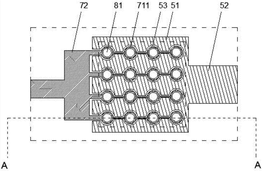
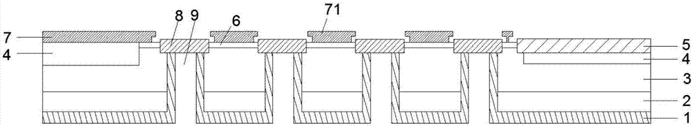
[0012] Such as figure 1 and image 3 As shown, this embodiment provides a matrix-arranged annular FET device, which includes a substrate 2, a buffer layer 3, and a barrier layer 6 from bottom to top; it also includes an annular isolation region 4, a gate 7, a source 8, and a drain 5. The annular isolation region 4 is formed on the surface of the barrier layer 6 and extends to the inside of the buffer layer 3, such as figure 1 As shown, between the two dotted lines is an annular isolation region 4; the source 8 is composed of 16 cylindrical source metals 81 arranged in a matrix, the array size is 4×4, and each source metal 81 is formed on the barrier Layer 6 extends above and bottom to buffer layer 3 . The gate 7 includes a first surrounding portion 71 and a first extending portion 72. The first surrounding portion 71 is composed of 16 closed rings 711 arranged in a matrix. The closed rings 711 are closed circular rings. The closed rings 711 and the source metal 81 One corre...

Embodiment 2

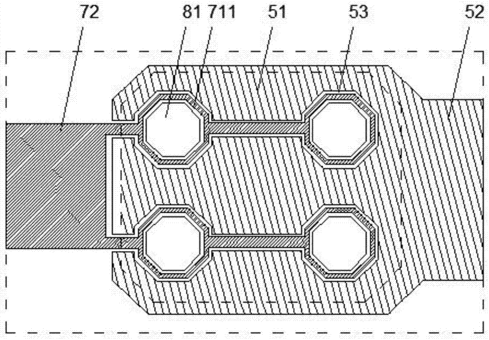
[0015] Such as figure 2 As shown, the source 8 of this embodiment is composed of four cylindrical source metals 81 arranged in a matrix, and the array size is 2×2; the first surrounding part 71 of the gate 7 is composed of four closed rings arranged in a matrix 711, the cross section of the closed ring 711 is a regular octagon; the second surrounding part 51 of the drain 5 has four through holes 53 arranged in a matrix, and the through holes 53 are regular octagonal holes; the outer part of the second surrounding part 51 The edge is an open octagon, and two openings are opened on one side of the second surrounding portion 51 ; four back holes 9 are opened upward from the bottom of the substrate 2 to the source metal 81 . Other structures are the same as in Embodiment 1.


PUM


Abstract

The invention relates to the technical field of semiconductor devices, and particularly relates to an annular field effect transistor (FET) device in matrix arrangement. From bottom to top, the annular FET device comprises a substrate, a buffer layer and a barrier layer, wherein an annular isolation area is formed on the surface of the barrier layer and extends into the interior of the buffer layer, a source electrode comprises a plurality of source electrode metals in matrix arrangement, a first surrounding part of a gate electrode comprises a plurality of closed rings in matrix arrangement, the closed rings surround corresponding source electrode metals, a first extending part extends from a closed ring at the edge of each row in a first straight line direction and covers the annular isolation area, a second surrounding part of a leakage electrode has a plurality of through holes in matrix arrangement, the closed ring is in corresponding through hole, a second extending part extends from a second surrounding part in a second straight line direction and covers the annular isolation area, the substrate is provided with a plurality of back holes from bottom up to the source electrode metal, and each source electrode metal passes through corresponding back hole and is connected with back metal through connection metal. Through adoption of the annular FET device in matrix arrangement, gate delay is lowered and breakdown voltage of the device is improved.

Description

technical field [0001] The invention belongs to the technical field of semiconductor devices, and in particular relates to a matrix-arranged annular FET device. Background technique [0002] The structural design of the die has a serious impact on the performance of the device. At present, the commonly used field effect transistor (FET) adopts a strip gate structure, and the source and drain are arranged on both sides of the gate. This kind of die design, with the same gate width, has a larger area, serious gate delay, and the uneven distribution of the electric field can easily lead to device breakdown. Contents of the invention [0003] The object of the present invention is to provide a matrix-arranged annular FET device that can reduce gate delay and increase breakdown voltage. [0004] In order to meet the above requirements, the technical solution adopted by the present invention is: provide a matrix-arranged annular FET device, which includes a substrate, a buffer ...

Claims


Application Information

Patent Timeline
Patent Type & Authority Applications(China)
IPC IPC(8): H01L29/417H01L29/423H01L29/78
CPCH01L29/41725H01L29/41775H01L29/42356H01L29/78
Inventor 李春江翟媛
Owner CHENGDU HIWAFER SEMICON CO LTD
Features
  • R&D
  • Intellectual Property
  • Life Sciences
  • Materials
  • Tech Scout
  • Unparalleled Data Quality
  • Higher Quality Content
  • 60% Fewer Hallucinations
Learn More