Supercharge Your Innovation With Domain-Expert AI Agents!

Circuit board and circuit board manufacturing method

A circuit board and inductor technology, which is applied in the fields of printed circuit manufacturing, printed circuit, printed circuit, etc., can solve the problems of increased noise in the final product, large solder paste resistance, and low production efficiency, so as to increase the resonance frequency and shorten the process , the effect of improving production efficiency

Active Publication Date: 2019-12-03
QING DING PRECISION ELECTRONICS HUAIAN CO LTD +2
View PDF4 Cites 0 Cited by
  • Summary
  • Abstract
  • Description
  • Claims
  • Application Information

AI Technical Summary

Problems solved by technology

However, soldering inductance components by welding makes the process lengthy and the production efficiency is low, and because the resistance value of the solder paste is larger than that of the wire material of the circuit board, the noise of the final product increases

Method used


Image

  • Circuit board and circuit board manufacturing method
  • Circuit board and circuit board manufacturing method
  • Circuit board and circuit board manufacturing method

Examples


Embodiment Construction

[0014] The circuit board and the manufacturing method of the circuit board provided by the present invention will be described in detail below in conjunction with specific implementation methods.

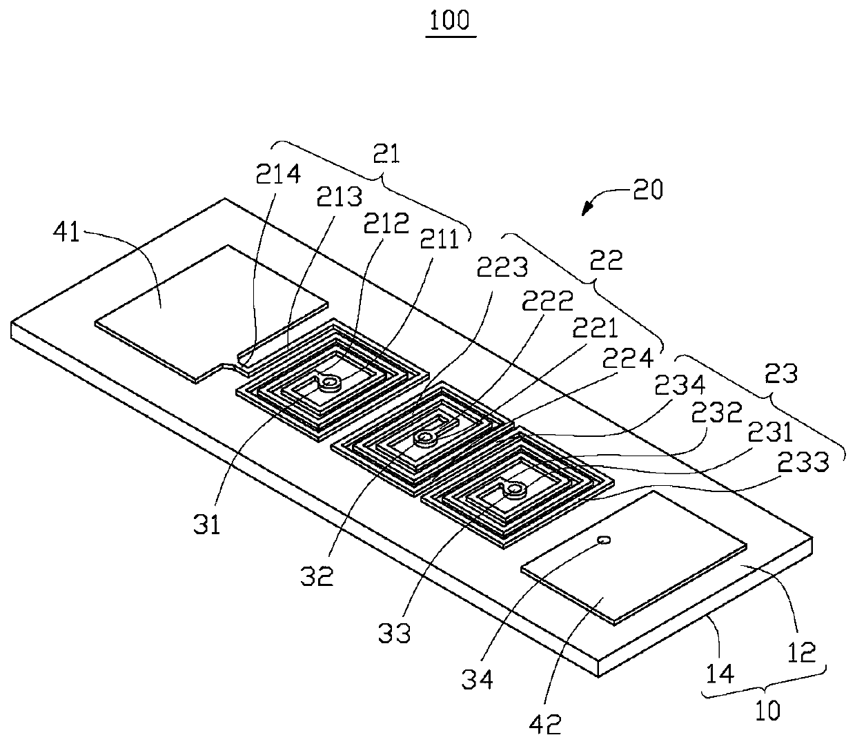
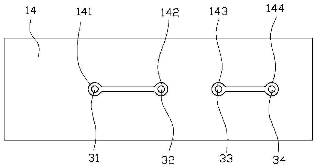
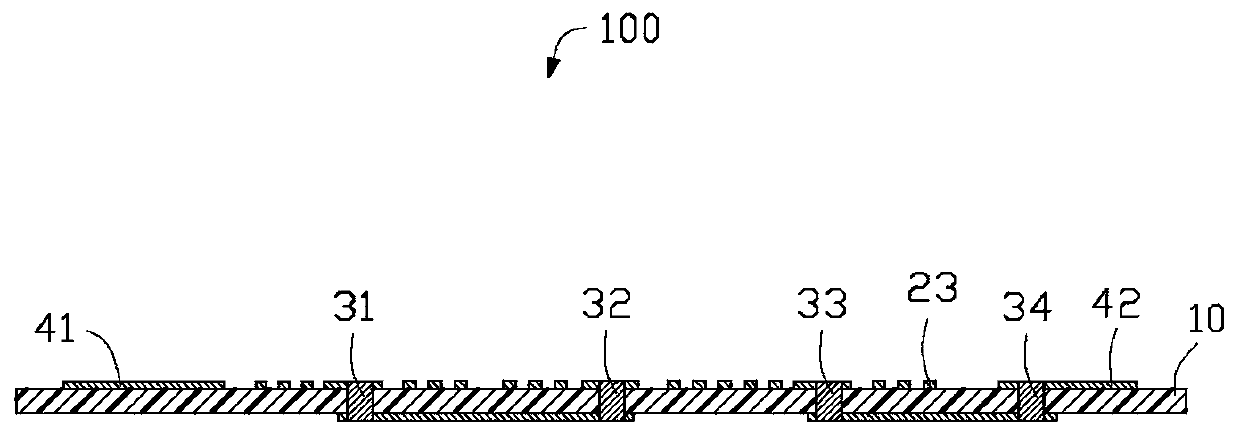
[0015] see figure 1 , the circuit board 100 provided by the embodiment of the present invention. The circuit board 100 includes a base 10 . The substrate 10 includes a first surface 12 and a second surface 14 . The first surface 12 and the second surface 14 are located on opposite sides of the base 10 . The first surface is provided with an inductor unit 20 .

[0016] The inductance unit 20 includes a first inductance coil 21 , a second inductance coil 22 and a third inductance coil 23 . In this embodiment, the first induction coil 21 , the second induction coil 22 and the third induction coil 23 are arranged side by side on the first surface 12 . Wherein, the first induction coil 21 is spaced apart from the second induction coil 22 , and the second induction coil 22 is electri...


PUM


Abstract

The invention relates to a manufacture method of a circuit board. The manufacture method comprises the steps of forming a first via, a second via, and a third via in a substrate; and selectively etching to remove a part of a first copper foil layer, so as to form a first inductive coil, a second inductive coil, and a third inductive coil, wherein the first inductive coil and the second inductive coil are electrically connected through the first via and the second via penetrating through the substrate, the second inductive coil and the third inductive coil are electrically connected through wires at the ends of the coils, the first inductive coil surrounds the first via and is introduced inwards coil by coil to the first via, the second inductive coil surrounds the second via and is introduced inwards coil by coil to the second via, and the third inductive coil surrounds the third via and is introduced inwards coil by coil to the third via.

Description

technical field [0001] The invention relates to a circuit board and a method for manufacturing the circuit board, in particular to a circuit board with an inductance unit and a method for manufacturing the circuit board with the inductance unit. Background technique [0002] At present, various antennas, such as Wireless Fidelity (Wi-Fi), Blue teeth, GlobalPositioning System (GPS), Near Field Communication (NFC), Code Division Multiple Access (CDMA), Long Term Evolution (LTE), etc. Both need to install inductance components on corresponding circuit boards. At present, the required inductance components are usually welded to the circuit board through solder paste by way of punching. However, soldering inductance components by bonding makes the process lengthy and the production efficiency is low, and because the resistance value of the solder paste is larger than that of the wire material of the circuit board, the noise of the final product increases. In addition, the induc...

Claims


Application Information

Patent Timeline
Patent Type & Authority Patents(China)
IPC IPC(8): H05K1/16H05K3/40
CPCH05K1/165H05K3/4046H05K2201/09654
Inventor 胡先钦沈芾云何明展庄毅强
Owner QING DING PRECISION ELECTRONICS HUAIAN CO LTD
Features
  • R&D
  • Intellectual Property
  • Life Sciences
  • Materials
  • Tech Scout
  • Unparalleled Data Quality
  • Higher Quality Content
  • 60% Fewer Hallucinations
Learn More