Operational amplifier for performing offset voltage correction on output working point
What is AI technical title?
AI technical title is built by PatSnap AI team. It summarizes the technical point description of the patent document.
An operational amplifier, offset voltage technology, applied in the field of operational amplifiers, can solve problems such as poor accuracy
Active Publication Date: 2017-11-14
西安华泰半导体科技有限公司
View PDF7 Cites 4 Cited by
Summary
Abstract
Description
Claims
Application Information
AI Technical Summary
This helps you quickly interpret patents by identifying the three key elements:
Problems solved by technology
Method used
Benefits of technology
Problems solved by technology
[0004] The purpose of the present invention is to provide an operational amplifier that performs offset voltage correction for the output operating point, so as to solve the problem of poor precision when performing offset voltage calibration at the operating point required by the user
Method used
Image
Click on the blue label to locate the original text in one second.
Reading with bidirectional positioning of images and text.
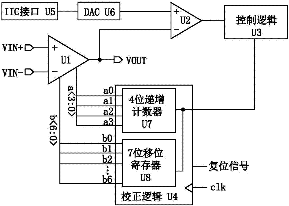
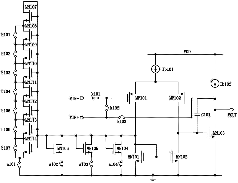
[0029] see figure 2, the non-inverting input end of the operational amplifier is connected to the gate of the PMOS transistor MP102 through the switch k103, the inverting input end is connected to the gate of the PMOS transistor MP101 through the switch k101, one end of the switch k102 is connected to the gate of...
Embodiment 2
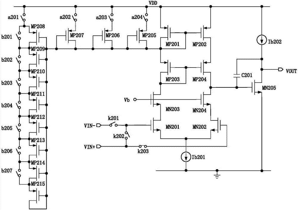
[0035] The structure of the operational amplifier in this embodiment is the same as that in Embodiment 1, and the gain stage in the main module of the operational amplifier is replaced with a telescopic operational amplifier structure.
PUM
Abstract
The invention relates to an operational amplifier for performing offset voltage correction on an output working point. The operational amplifier comprises an operational amplifier module, a comparator module, a logic control module, a correction logic module, an inter-integrated circuit (IIC) interface and a digital-to-analogue converter (DAC) module, wherein the IIC interface is connected with the DAC module, and an output end of the DAC module is connected with an in-phase input end of the comparator module; an inverting input end of the comparator module is connected with an output end (VOUT) of the operational amplifier module; an input end of the logic control module is connected with an output end of the comparator module; an output end of the logic control module is connected with an input end of the correction logic module. An offset correction process of the operational amplifier comprises coarse adjustment and fine adjustment; the coarse adjustment is carried out in a way of transistor parallel connection, and the fine adjustment is carried out in a way of transistor series connection, so that the correction accuracy is improved.
Description
technical field [0001] The invention belongs to the field of CMOS process integrated circuits, and in particular relates to an operational amplifier for correcting offset voltage for an output operating point. Background technique [0002] In the manufacturing process of the operational amplifier, due to the uncertainty of the CMOS manufacturing process and the mechanical pressure in the packaging process, the prepared operational amplifier inevitably has a certain offset voltage. As a result, when the amplifier is working normally, an unexpected error will always be superimposed on its output, which will inevitably have a certain impact on the performance of the entire circuit, especially the accuracy, especially in applications with small DC signals and high precision. There are many techniques to reduce or correct this offset voltage. Such as the use of larger transistors, self-zeroing and chopping techniques. During the correction process, it is necessary to add a comm...
Claims
Application Information
Patent Timeline
Application Date:The date an application was filed.
Publication Date:The date a patent or application was officially published.
First Publication Date:The earliest publication date of a patent with the same application number.
Issue Date:Publication date of the patent grant document.
PCT Entry Date:The Entry date of PCT National Phase.
Estimated Expiry Date:The statutory expiry date of a patent right according to the Patent Law, and it is the longest term of protection that the patent right can achieve without the termination of the patent right due to other reasons(Term extension factor has been taken into account ).
Invalid Date:Actual expiry date is based on effective date or publication date of legal transaction data of invalid patent.

