P-type silicon mother alloy production method

A silicon master alloy and a manufacturing method technology, which are applied in chemical instruments and methods, self-melt pulling method, crystal growth and other directions, can solve the problem of the large resistivity range of the master alloy, the large amount of boron dopant, and the resistivity grading. many problems, to achieve the effect of less resistivity binning, lower production costs, and lower dosage

Inactive Publication Date: 2017-12-01
JINKO SOLAR CO LTD +1
View PDF4 Cites 6 Cited by
  • Summary
  • Abstract
  • Description
  • Claims
  • Application Information

AI Technical Summary

Problems solved by technology

An example in the prior art is to obtain an N-type single crystal with uniform resistivity by the Czochralski method by melting N-type polysilicon raw materials containing phosphorus and boron, while in the prior art when making a P-type master alloy, only one One doping element boron, the resistivity range of the master alloy is large, the amount of boron dopant is large and the resistivity is divided into multiple levels, and the cost of the leveling is relatively high

Method used


Image

  • P-type silicon mother alloy production method

Examples


Embodiment Construction
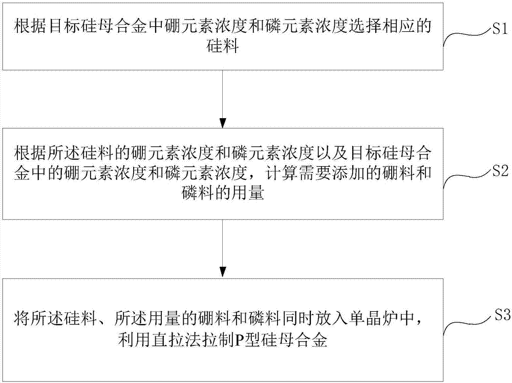
[0030] The core idea of ​​the present invention is to provide a method for making a P-type silicon master alloy, which can improve the uniformity of the resistivity of the P-type master alloy, reduce the amount of boron dopant, and reduce the resistivity into fewer stages, thereby reducing production costs.

[0031] The following will clearly and completely describe the technical solutions in the embodiments of the present invention with reference to the accompanying drawings in the embodiments of the present invention. Obviously, the described embodiments are only some, not all, embodiments of the present invention. Based on the embodiments of the present invention, all other embodiments obtained by persons of ordinary skill in the art without making creative efforts belong to the protection scope of the present invention.

[0032] The preparation method of the first P-type silicon master alloy provided in the embodiment of the present application is as follows: figure 1 as s...


PUM


Abstract

The invention discloses a P-type silicon mother alloy production method, which comprises the steps of selecting a corresponding silicon material according to the boron element concentration and the phosphorus element concentration in target silicon mother alloy; calculating the amount of boron material and phosphorus material which are need to be added according to the boron element concentration and the phosphorus element concentration of the silicon material, and the boron element concentration and the phosphorus element concentration in the target silicon mother alloy; putting the silicon material, the amount of boron material and phosphorus material simultaneously into a single crystal furnace, and pulling to prepare the P-type silicon mother alloy by using a Czochralski method. The P-type silicon mother alloy production method can improve the uniformity of the P-type mother alloy resistivity, reduce the amount of boron dopants and reduce the resistivity levels, thereby reducing the production cost.

Description

technical field [0001] The invention belongs to the technical field of photovoltaic cells, in particular to a method for preparing a P-type silicon master alloy. Background technique [0002] The master alloy in the photovoltaic industry refers to the alloy of the elements of the third or fifth group of the periodic table of chemical elements and silicon, mainly including boron-silicon alloys and phosphorus-silicon alloys. The role of the master alloy is to dope the polycrystalline silicon material, thereby changing the impurity concentration of the donor impurity (such as phosphorus) or the acceptor impurity (such as boron) in the silicon, so that the resistivity of the grown single crystal or polycrystalline silicon can meet the predetermined requirements. An example in the prior art is to obtain an N-type single crystal with uniform resistivity by the Czochralski method by melting N-type polysilicon raw materials containing phosphorus and boron, while in the prior art whe...

Claims


Application Information

Patent Timeline
IPC IPC(8): C30B15/04C30B29/06
CPCC30B15/04C30B29/06
Inventor 彭瑶苏勇邱建峰王义斌周慧敏
Owner JINKO SOLAR CO LTD
Why Eureka
Try Eureka