Test method and system of control storage chip
A memory chip and testing method technology, applied in error detection/correction, detection of faulty computer hardware, function inspection, etc., can solve the problem that memory interface control module access cannot be finely controlled, cannot be accurately predicted, and processing instruction logic is complex, etc.
- Summary
- Abstract
- Description
- Claims
- Application Information
AI Technical Summary
Problems solved by technology
Method used
Image

Examples
Embodiment 1
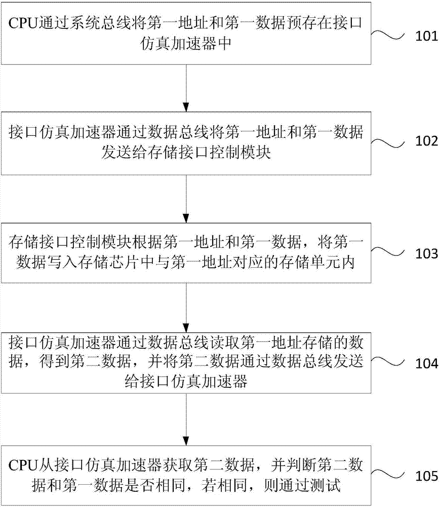
[0091] figure 1 A schematic flowchart of a method for controlling a memory chip test provided by an embodiment of the present invention, the method can be executed by a memory interface control module controlling a memory chip test system, wherein the system can be implemented by hardware and / or software , including the following steps:
[0092] Step 101, the CPU pre-stores the first address and the first data in the interface emulation accelerator through the system bus.
[0093] In this embodiment, for example, the CPU may be an ARM processor (Acorn RISC Machine). The ARM processor is a 32-bit RISC processor architecture that is widely used in many embedded system designs. It should be noted that the CPU is connected to the bus system through the instruction bus, the system bus and the data bus, and the interface emulation accelerator is connected to the bus system through the system bus to realize the connection between the interface emulation accelerator and the CPU. Th...
Embodiment 2
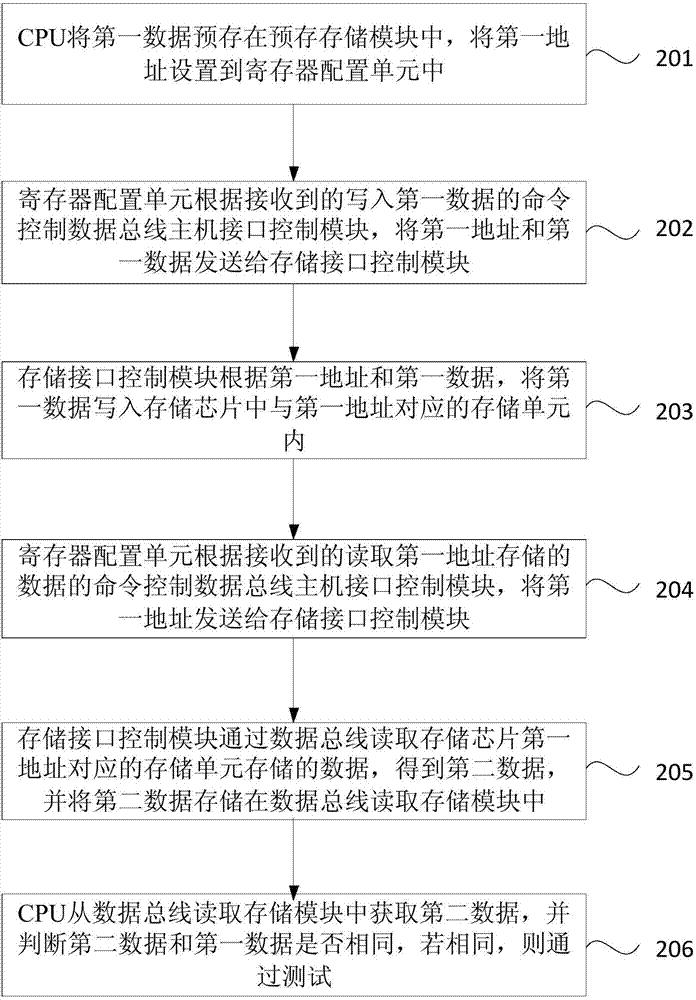
[0106] figure 2 It is a schematic flowchart of a testing method for controlling a memory chip provided by an embodiment of the present invention. On the basis of the above-mentioned embodiments, this embodiment further refines the interface simulation accelerator. The interface simulation accelerator includes a pre-stored storage module, a register configuration unit, a data bus host interface control module and a data bus read storage module, such as figure 2 As shown, the method specifically includes the following steps:
[0107] Step 201, the CPU pre-stores the first data in the pre-storage storage module, and sets the first address in the register configuration unit.
[0108] The pre-stored storage module is exemplified by Static Random Access Memory (SRAM), which is a kind of memory with static access function, and can save the data stored in it without refreshing circuit. The advantages of SRAM are high performance and low power consumption.
[0109] Step 202, the r...
Embodiment 3
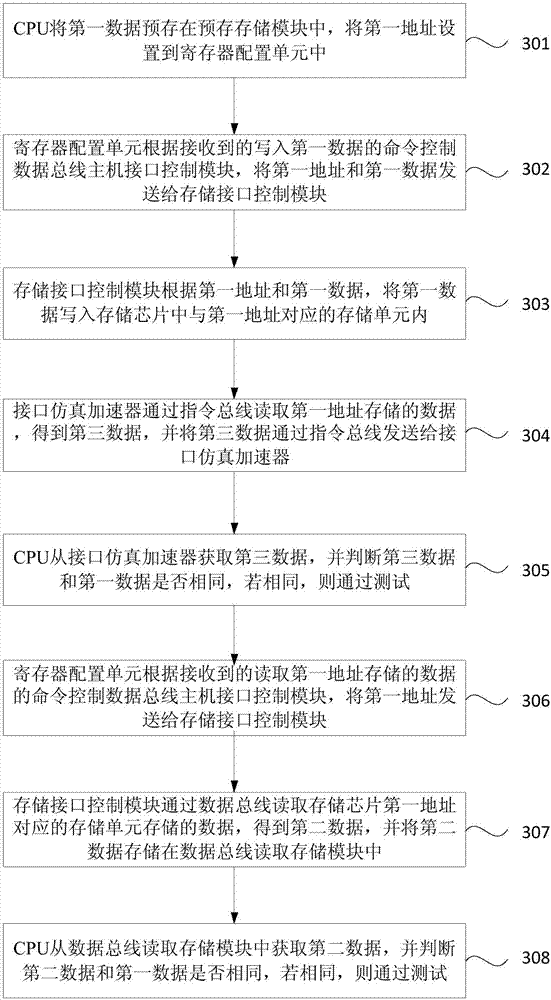
[0117] image 3 It is a schematic flowchart of a testing method for controlling a memory chip provided by an embodiment of the present invention. In this embodiment, on the basis of the above embodiments, the storage interface control module writes the first data into the memory chip corresponding to the first address according to the first address and the first data. After the steps in the storage unit, it also includes a transmission process between the interface emulation accelerator and the storage interface control module through the instruction bus. Such as image 3 As shown, the method includes the following steps:
[0118] Step 301, the CPU pre-stores the first data in the pre-storage storage module, and sets the first address in the register configuration unit.
[0119] Step 302, the register configuration unit controls the data bus host interface control module according to the received command to write the first data, and sends the first address and the first dat...
PUM
 Abstract
Description
Claims
Application Information
 - R&D
- Intellectual Property
- Life Sciences
- Materials
- Tech Scout
- Unparalleled Data Quality
- Higher Quality Content
- 60% Fewer Hallucinations
Browse by: Latest US Patents, China's latest patents, Technical Efficacy Thesaurus, Application Domain, Technology Topic, Popular Technical Reports.
© 2025 PatSnap. All rights reserved.Legal|Privacy policy|Modern Slavery Act Transparency Statement|Sitemap|About US| Contact US: help@patsnap.com