Pixel circuit, driving method of pixel circuit, organic light-emitting display panel and display device

A pixel circuit and light-emitting device technology, applied in circuits, electrical components, static indicators, etc., can solve problems such as inconsistent brightness of the first frame, and achieve the effects of avoiding afterimage phenomenon, avoiding parasitic capacitance, and reducing writing time

Active Publication Date: 2017-12-08
WUHAN TIANMA MICRO ELECTRONICS CO LTD +1
View PDF4 Cites 40 Cited by
  • Summary
  • Abstract
  • Description
  • Claims
  • Application Information

AI Technical Summary

Problems solved by technology

[0004] Embodiments of the present invention provide a pixel circuit, its driving method, an organic light-emitting display panel, and a display device, which are used to improve the problem of afterimage existing in the existing pixel circuit and the brightness inconsistency of the first frame after switching between high and low gray scales.

Method used


Image

  • Pixel circuit, driving method of pixel circuit, organic light-emitting display panel and display device
  • Pixel circuit, driving method of pixel circuit, organic light-emitting display panel and display device
  • Pixel circuit, driving method of pixel circuit, organic light-emitting display panel and display device

Examples


Embodiment 1

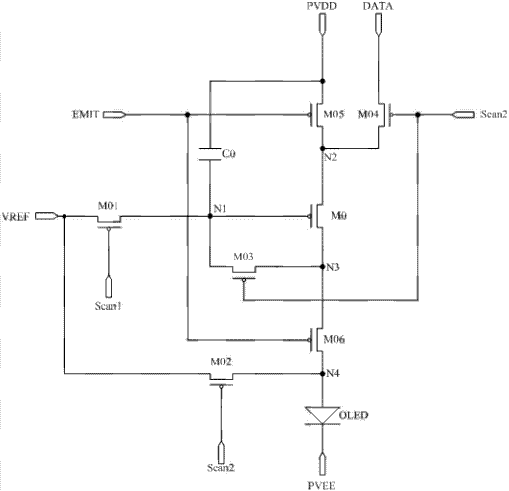
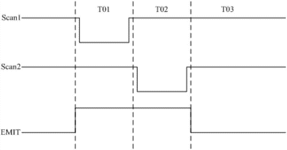
[0114] by Figure 4A Take the pixel circuit shown as an example, and the corresponding input timing diagram is as follows Figure 6A shown. Specifically, the main selection of Figure 6A The four stages T1, T2, T3 and T4 in the input timing diagram shown.

[0115] In the T1 stage, Scan1=0, CS1=1, CS2=1, Scan2=1, EMIT=1.

[0116] Since Scan1=0, the fourth transistor M4 is turned on and provides the reference voltage signal to the first node N1 and the second node N2, so that the voltages of the first node N1 and the second node N2 are both the voltage V of the reference voltage signal ref , to initialize the control electrode M0 and the first electrode of the driving transistor M0. Since CS1=1, the first transistor M1 is turned off. Since CS2=1, the second transistor M2 is turned off. Since Scan2=1, the fifth transistor M5 is turned off. Since EMIT=1, both the sixth transistor M6 and the seventh transistor M7 are turned off, and the light emitting device L does not emit ...

Embodiment 2

[0125] by Figure 4D Take the pixel circuit shown as an example, and the corresponding input timing diagram is as follows Figure 6B shown. Specifically, the main selection of Figure 6B The four stages T1, T2, T3 and T4 in the input timing diagram shown.

[0126] In the T1 stage, Scan1=0, CS1=1, Scan2=1, EMIT=1.

[0127] Since Scan1=0, the fourth transistor M4 is turned on and provides the reference voltage signal to the first node N1 and the second node N2, so that the voltages of the first node N1 and the second node N2 are both the voltage V of the reference voltage signal ref , to initialize the control electrode M0 and the first electrode of the driving transistor M0. Since CS1=1, the first transistor M1 is turned off, and the second transistor M2 is turned on. Since Scan2=1, both the third transistor M3 and the fifth transistor M5 are turned off. Since EMIT=1, both the sixth transistor M6 and the seventh transistor M7 are turned off, and the light emitting device ...

Embodiment 3

[0136] by Figure 5A Take the pixel circuit shown as an example, and the corresponding input timing diagram is as follows Figure 6C shown. Specifically, the main selection of Figure 6C The four stages T1, T2, T3 and T4 in the input timing diagram shown. and Figure 6C In Scan3_1 represents Figure 5A The signal of the third scan signal terminal Scan3 in the pixel circuit shown.

[0137] In the T1 phase, since Scan3_1=0, the eighth transistor M8 is turned on and provides the reference voltage signal to the first terminal of the light-emitting device L, so as to reset the light-emitting device L, so as to avoid the problem of light emission in the previous frame and light emission in the current frame. influences. In the T2-T4 phase, since Scan3_1=1, the eighth transistor M8 is turned off. The working processes of the other transistors are basically the same as those of the transistors in the T1-T4 phases in the first embodiment, and will not be repeated here.

[0138]...


PUM


Abstract

The invention discloses a pixel circuit, a driving method of the pixel circuit, an organic light-emitting display panel and a display device. A unified public voltage signal is inputted to a first electrode of a drive transistor before a data signal is written into a control electrode of the drive transistor; the public voltage signal and a threshold voltage of the drive transistor are written into a control electrode of the drive transistor, so that relatively high current can pass through the drive transistor, threshold voltage deviation, which is caused by bias stress, of the drive transistor can be recovered, a retarding effect of the drive transistor can be improved and the occurrence of a ghosting phenomenon can be prevented; in addition, when the data signal is written into the control electrode of the drive transistor, a time of writing the data signal can be shortened, and the control electrode and the first electrode of the drive transistor can achieve jump through a unified potential, so that a difference, which is caused by stray capacitance between the control electrode and the first electrode of the drive transistor, can be prevented, the problem that threshold voltage grabbing is inconsistent due to voltage jump can be avoided and consistent brightness of the first frame after high-low grayscale switching can be guaranteed.

Description

technical field [0001] The present invention relates to the field of display technology, in particular to a pixel circuit, a driving method thereof, an organic light-emitting display panel and a display device. Background technique [0002] Organic Light Emitting Diode (OLED) display is one of the hotspots in the field of flat panel display research today. Compared with liquid crystal display, OLED has the advantages of low energy consumption, low production cost, self-illumination, wide viewing angle and fast response speed. Currently, in the field of flat panel displays such as mobile phones, PDAs, and digital cameras, OLEDs have begun to replace traditional Liquid Crystal Displays (LCDs). Among them, pixel circuit design is the core technical content of OLED display, which has important research significance. [0003] An existing pixel circuit structure, such as figure 1 As shown, it includes 6 transistors: M01-M06, 1 driving transistor M0 and 1 capacitor C0. figure 1 ...

Claims


Application Information

Patent Timeline
Patent Type & Authority Applications(China)
IPC IPC(8): G09G3/3225
CPCG09G3/3225G09G2320/0257H10K59/12G09G3/3233G09G2300/0819G09G2300/0842G09G2300/0861G09G2320/0214H10K50/805G09G3/3258
Inventor 李玥朱仁远向东旭高娅娜陈泽源蔡中兰
Owner WUHAN TIANMA MICRO ELECTRONICS CO LTD
Why Eureka
Try Eureka