Semiconductor memory device
A memory and semiconductor technology, applied in static memory, digital memory information, information storage, etc., can solve problems such as increased difficulty in wiring
- Summary
- Abstract
- Description
- Claims
- Application Information
AI Technical Summary
Problems solved by technology
Method used
Image

Examples
Embodiment Construction
[0052] What is described in this chapter is the best way to implement the present invention. The purpose is to illustrate the spirit of the present invention rather than to limit the protection scope of the present invention. The protection scope of the present invention should be determined by the claims. In order to make the features and advantages of the present invention more comprehensible, preferred embodiments thereof are specifically cited below and described in detail with accompanying drawings.
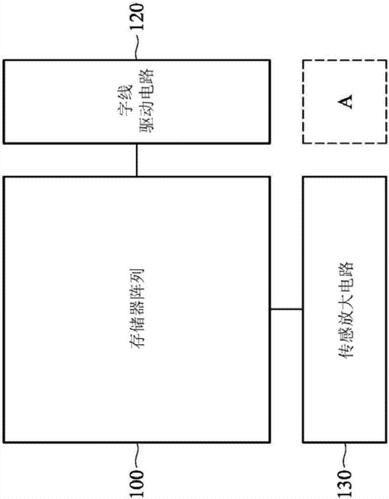
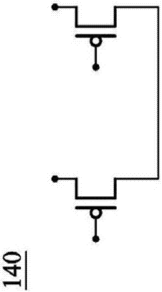
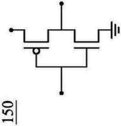
[0053] image 3 is a block diagram of a semiconductor memory device 300 according to an embodiment of the present invention. The semiconductor memory device 300 includes a plurality of memory arrays 310-1...310-N, word line driving circuits 320-1...320-N, and a plurality of sense amplifier circuits 330-1...330-N, wherein N is a positive integer. In the embodiment of the present invention, in image 3 The transistors included in the control circuit included in each region ...
PUM
 Abstract
Description
Claims
Application Information
 - R&D
- Intellectual Property
- Life Sciences
- Materials
- Tech Scout
- Unparalleled Data Quality
- Higher Quality Content
- 60% Fewer Hallucinations
Browse by: Latest US Patents, China's latest patents, Technical Efficacy Thesaurus, Application Domain, Technology Topic, Popular Technical Reports.
© 2025 PatSnap. All rights reserved.Legal|Privacy policy|Modern Slavery Act Transparency Statement|Sitemap|About US| Contact US: help@patsnap.com