
Enhanced layout of multiple-finger electrostatic discharge (ESD) protection device

An ESD protection and protection device technology, applied in circuits, electrical components, electrical solid devices, etc., can solve problems such as the inability to protect on-voltage semiconductor devices

Pending Publication Date: 2017-12-08
INTERSIL INC
View PDF4 Cites 0 Cited by
  • Summary
  • Abstract
  • Description
  • Claims
  • Application Information

AI Technical Summary

Problems solved by technology

However, existing bipolar and MOSFET based clamps for ESD protection cannot protect any semiconductor device with a turn-on voltage lower than the trigger voltage of the ESD clamp used

Method used


Image

  • Enhanced layout of multiple-finger electrostatic discharge (ESD) protection device
  • Enhanced layout of multiple-finger electrostatic discharge (ESD) protection device
  • Enhanced layout of multiple-finger electrostatic discharge (ESD) protection device

Examples


Embodiment Construction

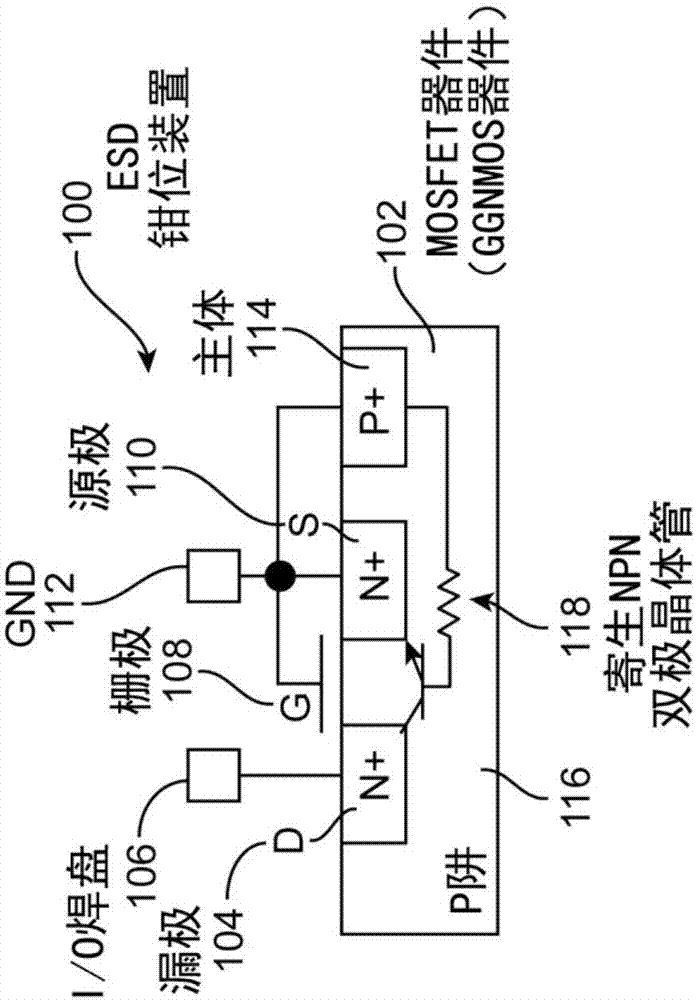
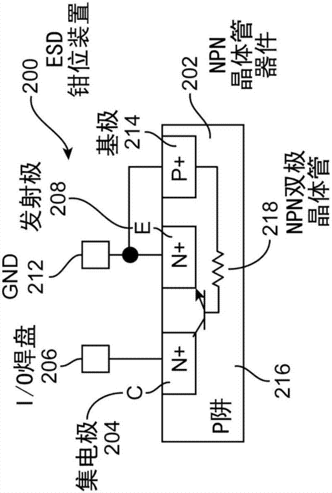
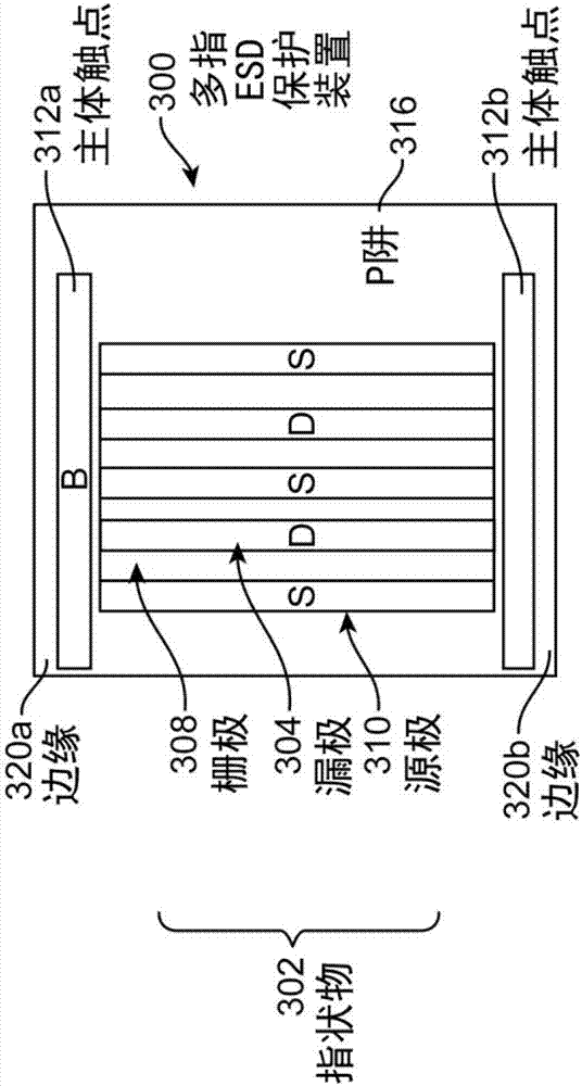
[0015] The present embodiments will now be described in detail with reference to the accompanying drawings, which are provided as illustrative examples of the embodiments to enable those skilled in the art to practice embodiments and alternatives that will be apparent to those skilled in the art. It is worth noting that the following figures and examples are not meant to limit the scope of embodiments of the present invention to a single embodiment, but other embodiments may be realized by exchanging some or all of the described or illustrated elements . Furthermore, where certain elements of the present embodiment can be partially or fully realized using known components, only those parts of these known components necessary for understanding the present embodiment will be described, and the description of other parts of these known components will be described. A detailed description will be omitted so as not to obscure the present embodiment. Embodiments described as implem...


PUM


Abstract

An enhanced layout for a multiple-finger ESD protection device has several embodiments. In these embodiments, the base contacts of the NPN (or PNP) transistors utilized as voltage clamps in the multiple-finger NPN-based (or PNP-based) multiple-finger ESD protection device are disposed at opposite edges of the multiple-finger ESD protection device and oriented perpendicularly to the orientation of the fingers in the multiple-finger ESD protection device. Similarly, the body contacts of the NMOS (or PMOS) transistors utilized as voltage clamps in the multiple-finger NMOS-based (or PMOS-based) multiple-finger ESD protection device are disposed at opposite edges of the multiple-finger ESD protection device and oriented perpendicularly to the orientation of the fingers in the multiple-finger ESD protection device.

Description

[0001] Cross References to Related Applications [0002] This application claims priority to U.S. Provisional Patent Application Serial No. 62 / 327,726, filed April 26, 2016, and U.S. Provisional Patent Application Serial No. 62 / 478,461, filed March 29, 2017, the entire contents of which applications are incorporated by reference Incorporated into this article. technical field [0003] The present embodiments relate generally to electrostatic discharge (ESD) protection, and more particularly to enhanced layout of ESD protection devices for integrated circuits. Background technique [0004] Metal Oxide Semiconductor Field Effect Transistor (MOSFET) and Bipolar Junction Transistor (BJT) devices are commonly used for electrostatic discharge (ESD) protection in CMOS integrated circuits to clamp any large ESD induced voltage pulses to a sufficiently low level to avoid damage to the semiconductor devices and / or metal interconnections in the integrated circuit chip involved. Howev...

Claims


Application Information

Patent Timeline
IPC IPC(8): H01L27/02H01L23/62
CPCH01L23/62H01L27/0251H01L27/0292H01L27/027H01L27/0259H01L27/0266H01L29/1095H01L21/823475H01L21/8222H01L29/42304H01L27/0207
Inventor 阿布·T·卡比尔
Owner INTERSIL INC
Learn More