Current detection circuit including electrostatic capacitor and rectifying element for increasing gate voltage of protecting mosfet

a current detection circuit and gate voltage technology, applied in the direction of ac-dc conversion, measurement, pulse technique, etc., can solve the disadvantageous narrowing of the detection voltage range of the drain voltage of the power mosfet b>101/b>, and the reduction of current detection accuracy

Inactive Publication Date: 2011-10-13
PANASONIC CORP
View PDF4 Cites 32 Cited by
  • Summary
  • Abstract
  • Description
  • Claims
  • Application Information

AI Technical Summary

Benefits of technology

[0014]Accordingly, it is an object of the present invention to provide a current detection circuit capable of solving the above-mentioned problems, and including a power transistor having a first terminal and a second terminal, a sense transistor having a fourth terminal and a third terminal connected to the first terminal, an operational amplifier to make the voltage at the fourth terminal coincide with the voltage at the second terminal, and a protecting MOSFET for protecting the operational amplifier from an overvoltage. In particular, it is an object of the present invention to provide a current detection circuit capable of solving the above-mentioned problems, and capable of detecting a load current with an accuracy higher than that of the prior art with exercising negative feedback to a relatively high voltage by the operational amplifier while satisfying the withstand voltage between the source and the gate of the protecting MOSFET, even when the substrate bias effect occurs in the protecting MOSFET due to implementation of the current detection circuit with an integrated circuit.
[0035]With this arrangement, it is possible to apply a gate threshold voltage, which is increased by the substrate bias effect, to the gate of the MOSFET transistor in addition to the source voltage. Therefore, even when the substrate bias effect in the MOSFET transistor is relatively large, the load current can be detected with an accuracy higher than that of the prior art with exercising negative feedback to the relatively high voltage while satisfying the withstand voltage between the source and the gate of the MOSFET transistor.

Problems solved by technology

An excessive current applied to a load when abnormality occurs deteriorates or damages the load or the power transistor connected to the load.
This leads to such a problem that a detection voltage range of a drain voltage of the power MOSFET 101 is disadvantageously narrowed than a detection voltage range when there is no substrate bias effect.
As a result, there is caused such a problem that a current detection accuracy is reduced.

Method used


Image

  • Current detection circuit including electrostatic capacitor and rectifying element for increasing gate voltage of protecting mosfet
  • Current detection circuit including electrostatic capacitor and rectifying element for increasing gate voltage of protecting mosfet
  • Current detection circuit including electrostatic capacitor and rectifying element for increasing gate voltage of protecting mosfet

Examples


first preferred embodiment

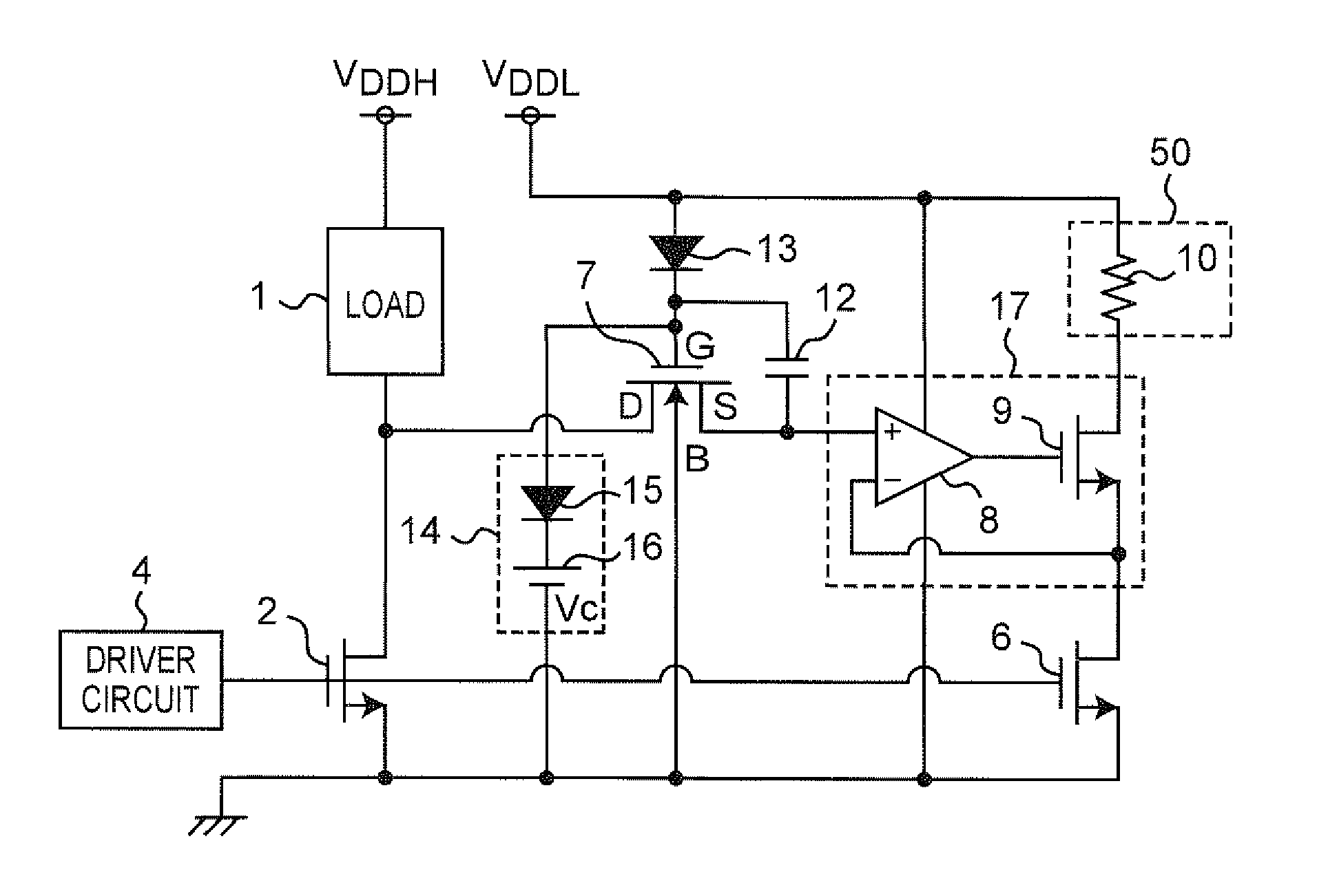
[0046]FIG. 1 is a circuit diagram of a current detection circuit according to the first preferred embodiment of the present invention. Referring to FIG. 1, the current detection circuit of the present preferred embodiment is an integrated circuit, and constituted by including a load 1, a power transistor 2, a sense transistor 6, a voltage control circuit 17 including an operational amplifier 8 and an output transistor 9, a detector circuit 50 including a resistor 10, a protecting MOSFET 7, a diode 13, an electrostatic capacitor 12, a voltage clamp circuit 14 including a diode 15 and a DC voltage source 16, and a driver circuit 4.

[0047]As described in detail later, the current detection circuit of the present preferred embodiment is characterized by including:

[0048](a) the power transistor 2 having a source, a drain and a gate, where a current flowing between the source thereof and the drain thereof is controlled by a control voltage applied to the gate thereof;

[0049](b) the sense tr...

first modified preferred embodiment

of First Preferred Embodiment

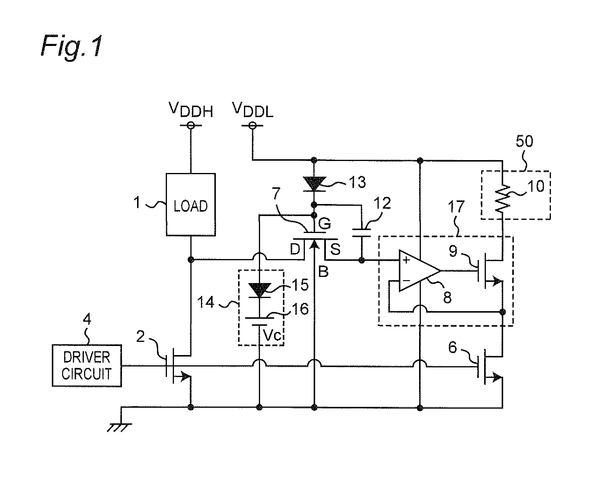
[0068]FIG. 2 is a circuit diagram of a current detection circuit according to the first modified preferred embodiment of the first preferred embodiment of the present invention. The present modified preferred embodiment is different from the first preferred embodiment in that a voltage clamp circuit 14A is provided in place of the voltage clamp circuit 14. Referring to FIG. 2, the voltage clamp circuit 14A is configured to include the diode 15 and the DC voltage source 16. In this case, the diode 15 has the anode connected to the gate of the protecting MOSFET 7 and the cathode connected to a voltage source, which outputs a power voltage VDDLA, via the DC voltage source 16. In this case, the power voltage VDDLA has a sine waveform. In contrast to the first preferred embodiment in which the clamp voltage Vc of the voltage clamp circuit 14 is a fixed voltage generated relative to the ground potential of the reference electric potential, the clamp voltage Vc...

second modified preferred embodiment

of First Preferred Embodiment

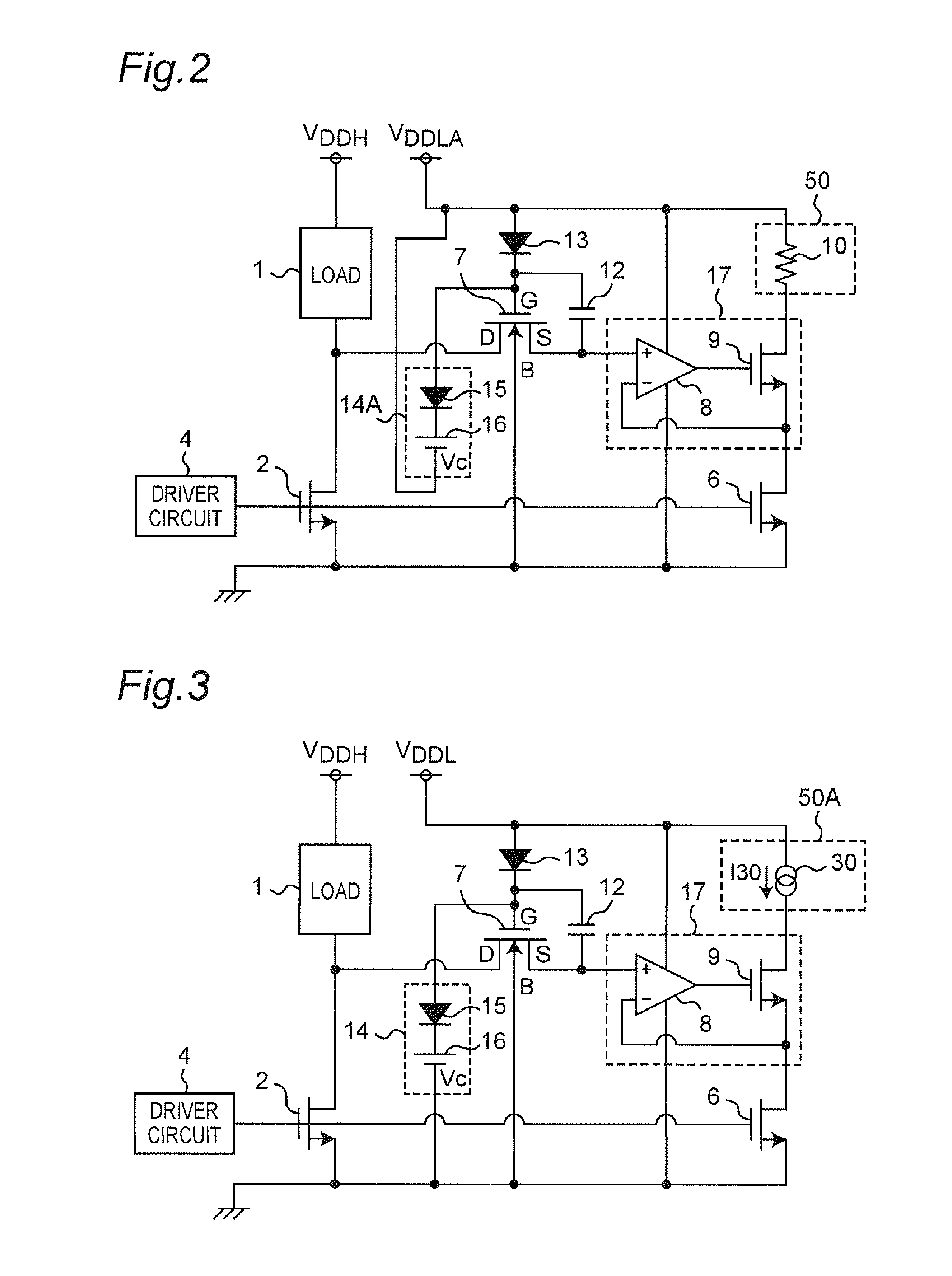
[0070]FIG. 3 is a circuit diagram of a current detection circuit according to the second modified preferred embodiment of the first preferred embodiment of the present invention. The present modified preferred embodiment is characterized in that a detector circuit 50A is provided in place of the detector circuit 50 as compared with the first preferred embodiment. In this case, the detector circuit 50A is configured to include a constant current source 30 that outputs a current having a constant current value I30. The constant current source 30 constitutes a current comparator. Referring to FIG. 3, the drain of the output transistor 9 is connected to the voltage source, which outputs the power voltage VDDL, via the constant current source 30. According to the present modified preferred embodiment, the drain voltage of the output transistor 9 decreases when the current value of the drain current of the sense transistor 6 is larger than the constant current...


PUM


Abstract

Using a electrostatic capacitor and a diode, a gate voltage of a protecting MOSFET is increased when a drain voltage of a power transistor increases. A voltage clamp circuit clamps the maximum voltage of the gate voltage of the protecting MOSFET to a predetermined clamp voltage. A voltage control circuit controls a drain voltage of a sense transistor so as to substantially coincide with a source voltage of the protecting MOSFET.

Description

[0001]The disclosure of Japanese Patent Application No. 2010-088724 filed Apr. 7, 2010 including specification, drawings and claims is incorporated herein by reference in its entirety.BACKGROUND OF THE INVENTION[0002]1. Field of the Invention[0003]The present invention relates to a current detection circuit for detecting a value of a current flowing through a power semiconductor device.[0004]2. Description of the Related Art[0005]Power semiconductor devices (referred to as power transistors hereinafter) such as thyristors are used for power conversion and power control. For example, the power semiconductor devices are often used as power control devices for use in driving devices for inverter control of motors, or power control devices for use in switching power supplies. Concretely speaking, a current flowing through a power transistor is used for generating a driving torque of a motor load. In the switching power supply, the power transistor is used for improving response of the s...

Claims


Application Information

Patent Timeline
Patent Type & Authority Applications(United States)
IPC IPC(8): G01R19/22
CPCH03K17/0822G01R19/0092H03K2217/0027
Inventor KUME, TOMOHIRO
Owner PANASONIC CORP
Why Eureka
Try Eureka