Optical Sensor Device And Method For Operating Time-of-flight Sensor

A technology of optical sensors and equipment, which is applied in the field of integrated circuits and optical sensors, and can solve problems such as difficult and large signal voltages

Active Publication Date: 2017-12-08
INFINEON TECH AG
View PDF7 Cites 7 Cited by
  • Summary
  • Abstract
  • Description
  • Claims
  • Application Information

AI Technical Summary

Problems solved by technology

Since this charge is small, it is difficult to obtain large signal voltages from electronic readout circuits relative to noise sources
[0003] Thus, current designs of time-of-flight sensors expose intrinsic limitations in signal quality, and thus in the accuracy of time-of-flight measurements

Method used


Image

  • Optical Sensor Device And Method For Operating Time-of-flight Sensor
  • Optical Sensor Device And Method For Operating Time-of-flight Sensor
  • Optical Sensor Device And Method For Operating Time-of-flight Sensor

Examples


Embodiment Construction

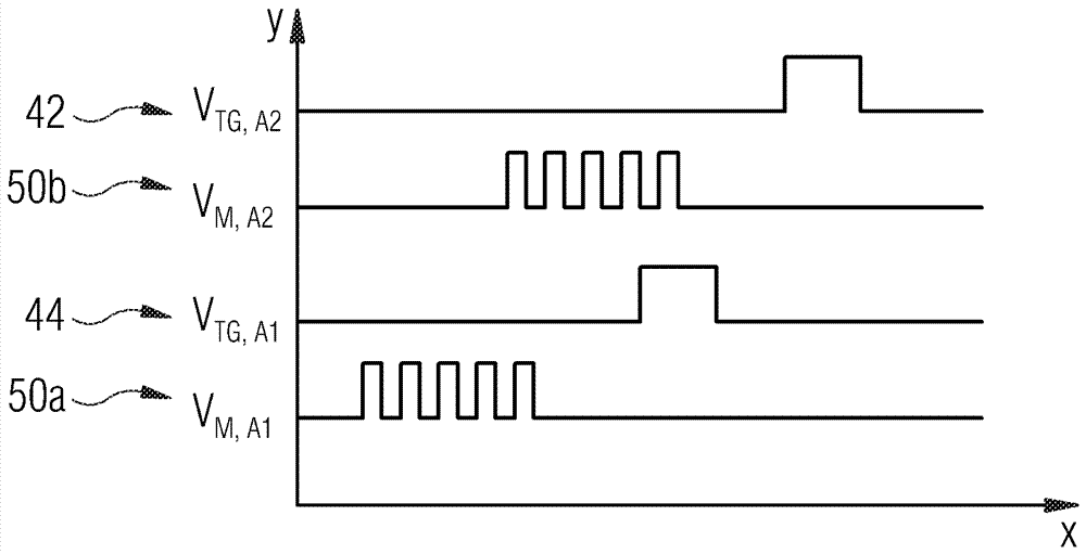
[0018] Hereinafter, embodiments of the present disclosure will be described in more detail. Elements shown in corresponding figures having the same or similar functions will have the same reference signs associated therewith. Furthermore, the same reference designation appended with a single letter (a, b, c, d) may refer to the same element in another pixel, where the same reference designation appended with an apostrophe (') may refer to the same element in the same pixel but The same element associated with different photogenerated charge carriers.

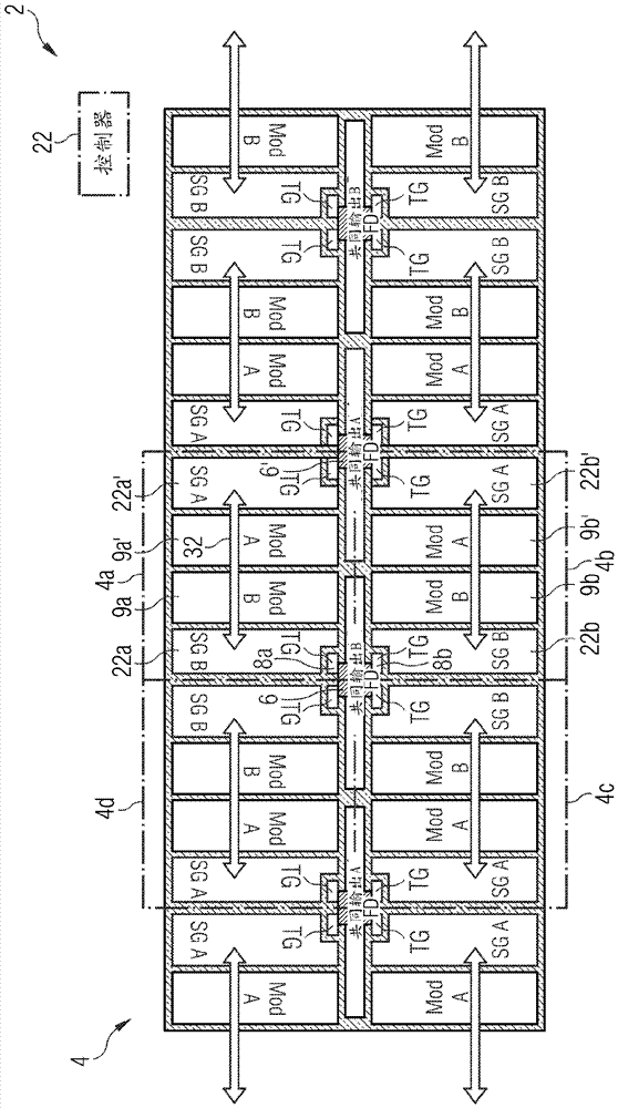
[0019] figure 1 A schematic plan view of the optical sensor device 2 is shown. The optical sensor device 2 may be a time-of-flight sensor. The sensor 2 comprises a pixel array 4, a readout node 6, a first transfer gate 8a and a second transfer gate 8b. The pixel array 4 has a plurality of pixels 4a, 4b. The readout node may be located at least between two pixels of the plurality of pixels such that both the first pixel 4 a ...


PUM


Abstract

The present invention discloses an optical sensor device and a method for operating a time-of-flight sensor. The optical sensor device, which may be a time-of-flight sensor, comprises a pixel array having a plurality of pixels. Moreover, the optical sensor device comprises a read-out node configured to provide photo-generated charge carriers from a first pixel and a second pixel for read-out and a first transfer gate configured to enable a read-out of the first pixel by using the read-out node and a second transfer gate to disable a read-out of the second pixel during read-out of the first pixel.

Description

technical field [0001] The present disclosure relates generally to the field of integrated circuits, and more particularly to the field of optical sensors employing photogate structures for redirection of photogenerated charge carriers and placement of photogate structures. Another embodiment shows a transmission gate light mixing device. Background technique [0002] Optical sensors for depth imaging and in particular time-of-flight optical sensors suffer from a relatively high (i.e. poor) signal-to-noise ratio for electrical signals representing time-of-flight, which is the time-of-flight from an electromagnetic signal such as, for example, light The time it takes for an active illumination source to travel to the object and then travel back or further forward to the light sensor. The signal can be formed by the amplitude modulation of the illumination source and the image relationship in the optical sensor. Depending on the phase relationship to the illumination source,...

Claims


Application Information

Patent Timeline
IPC IPC(8): H01L27/146G01S7/4914G01S17/00G01S17/894
CPCH01L27/14605H01L27/14609G01S7/4914H01L27/14614G01S17/894H04N25/778H04N25/77G01S17/00H04N25/767H04N25/75
Inventor H.法伊克
Owner INFINEON TECH AG
Why Eureka
Try Eureka